Summary
We are characterizing Si-based single-electron quantum dots at low temperatures (down to 10 mK) to explore the possibility of quantum coherent manipulation in Si-based technology.
Description

Devices based on moving and controlling single electrons offer the tantalizing possibility of achieving quantum information processing by virtue of their spin or charge coherent properties. We are pursuing CMOS-compatible Si-based quantum dots for a variety of goals, including:”
- Narrowband high-MHz or GHz reflectometry from the dots, for both noise measurements over 15 decades of frequency and probing quantum manipulation.
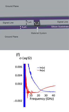
- Broadband GHz non-contact sensing of buried structures, ranging from AQS (analogue quantum simulation) structures made with single-atom precision to two-dimensional flakes with novel materials properties (e.g., twisted bilayer graphene).
- Transducing single electrons to single photons and back, for both metrology and quantum networking avenues.
Created July 14, 2015, Updated March 26, 2025

