
Official websites use .gov
A .gov website belongs to an official government organization in the United States.
Secure .gov websites use HTTPS
A lock (
) or https:// means you’ve safely connected to the .gov website. Share sensitive information only on official, secure websites.
NanoFab Tool: ThermoFisher Helios 5 FX Dual Beam Scanning Electron Microscope (SEM) and Focused Ion Beam (FIB)
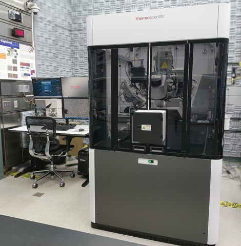
The ThermoFisher Helios 5 FX dual-beam microscope combines a monochromated field emission scanning electron microscope (FE-SEM) with an advanced focused ion beam (FIB) column for automated preparation of site-specific lamellae for Transmission Electron Microscopy (TEM) and Atom Probe Tomography (APT) instruments. Enhanced capabilities include chemical characterization using energy dispersive x-ray spectroscopy (EDS) and in-situ S/TEM imaging of lamellae. The tool supports substrates from small pieces (standard 10mm stubs, qty. 5) up to 70mm diameter.
Specifications/Capabilities
- FE-SEM
- Resolution: sub-nanometer from 1 kV to 15 kV.
- High resolution in-lens electron detectors with Through Lens (TLD, secondary and backscatter mode), In Column (ICD, low-loss backscatter) detectors.
- Scanning transmission electron microscopy (STEM 4) detector with bright-field (BF), dark-field (DF), and high-angle annular dark-field (HAADF) segments.
- Retractable dedicated backscatter detector with annular segments (ABS/CBS).
- Retractable T-Pix detector for zone axis alignment of lamella for STEM.
- CompuStage with alpha and beta tilt.
- Electron beam deceleration for 50 V effective landing voltage.
- Robotized load lock for automatic sample loading/unloading.
- Integrated plasma cleaner to minimize contamination.
- FIB (Ga+ ion source)
- High efficiency secondary ion detector.
- Electron flood gun for ion charge compensation.
- Secondary Ion imaging detector (ICE).
- Integrated beam current measurement for automatic milling/deposition recipe correction and consistent results.
- Real time monitoring of milling and deposition processes.
- End point monitoring for depth profile applications.
- Automated Easy Lift manipulator for removing transmission electron microscopy (TEM) and atom probe tomography (APT) samples.
- Enhanced capabilities for simultaneous materials characterization
- Energy dispersive x-ray spectroscopy Oxford Instruments Ultim Max 100 mm2 SDD-EDS detector (element characterization).
- Gas injection system chemistries
- Tungsten deposition.
- Platinum deposition.
- Carbon deposition.
- Selective carbon etch.
- Software packages
- MAPS – Automated large area imaging and stitching, correlative.
- Auto TEM – Automated TEM sample preparation including liftout.
- iFAST Developers kit.
- Auto Slice and View – Automated sequential milling and image capturing generates datasets for 3D reconstruction.
- Aztec – User-friendly EDS data collection and analysis software now with Live SEM capability.
- NanoBuilder – Advanced computer aided design (CAD) based patterning using GDSII files.
Usage Information
Supported Sample Sizes
- Maximum sample diameter: 70 mm.
- Small pieces supported: Yes.
- Non-magnetic materials: Yes.
- Biological materials: No.
- Radioactive materials: No.
Typical Applications
- Automated preparation of TEM lamellae (traditional, planar, ex-situ lift out).
- Sample preparation for atom probe tomography.
- Analysis and mapping of sample composition for site-specific TEM lamellae
- S/TEM in-situ imaging of thinned lamellae.
- Workflow for inverted TEM lamellae prep.