
Official websites use .gov
A .gov website belongs to an official government organization in the United States.
Secure .gov websites use HTTPS
A lock (
) or https:// means you’ve safely connected to the .gov website. Share sensitive information only on official, secure websites.
Manipulating Multiple Lasers on a Single Chip: Paving the Way for a New Generation of Quantum Devices
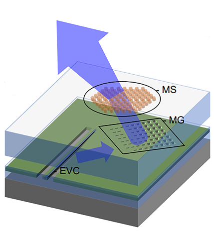
NIST researchers designed and fabricated this on-chip system to shape multiple laser beams (blue arrows) and control their polarization before the light is sent into space to interact with a device or material. Three components all contribute to manipulating the laser beams: An evanescent coupler (EVC), which couples light from one device to another; a metagrating (MG), a tiny surface imprinted with millions of tiny holes that scatter light just as a large-scale diffraction grating would; and a metasurface (MS), a small glass surface studded with millions of pillars that acts as lenses.
Researchers at the National Institute of Standards and Technology (NIST) have developed chip-scale devices for simultaneously manipulating the color, focus, direction of travel, and polarization of multiple beams of laser light.
The ability to tailor those properties using a single chip is essential for fabricating a new class of portable sensors that could measure such fundamental quantities as rotation, acceleration, time, and magnetic fields with unprecedented accuracy -- outside the confines of a laboratory.
Typically, a laboratory bench as big as a dining room table is required to house the assortment of lenses, polarizers, mirrors, and other apparatus required to manipulate even a single beam of laser light. Yet many quantum technologies, including miniature optical atomic clocks and some future quantum computers, will require simultaneous access to multiple, widely varying laser colors within a small region of space.
To tackle the problem, NIST scientist Vladimir Aksyuk and his colleagues combined two chip-scale technologies: Integrated photonic circuits, which use tiny transparent channels and other microscale components to guide light; and a source of unconventional optics known as an optical metasurface. Such surfaces consist of glass wafers imprinted with millions of tiny structures, only a few hundred billionths of a meter in height, that manipulate the properties of light without the need for bulky optics.
Aksyuk and his collaborators demonstrated that a single photonic chip did the work of 36 optical components, simultaneously controlling the direction, focus, and polarization (the plane in which a light wave vibrates as it travels) of 12 laser beams divided among four distinct colors.
The team also showed that the tiny chip can direct two beams of different colors to travel alongside each other, a requirement for some types of advanced atomic clocks.
“Replacing an optical table full of bulky optical components with a simple semiconductor wafer that can be fabricated in the clean room is truly game-changing,” said Amit Agrawal, a member of the NIST team. “These kinds of technologies are needed since they are robust and compact and can be easily reconfigured for different experiments under real-world conditions,” he added
The chip-based optical system is a work in progress, noted Aksyuk. For instance, the laser light is not yet powerful enough to cool atoms to the ultra-low temperatures required for a miniaturized advanced atomic clock. (Although laser light would ordinarily energize atoms, causing them to heat up and move faster, the opposite happens if the frequency and other properties of the light are chosen carefully. Upon striking the atoms, the laser photons induce the atoms to give up energy and cool down so that they can be trapped by a magnetic field.)
Even without the cooling capability, the miniature optical system “is a key stepping stone toward building an advanced atomic clock on a chip,” Aksyuk said.
He and his colleagues reported the findings in the April 3 issue of Light: Science and Applications.
Paper:
Chad Ropp, Wenqi Zhu, Alexander Yulaev, Daron Westly, Gregory Simelgor, Akash Rakholia, William Lunden, Dan Sheredy, Martin M. Boyd, Scott Papp, Amit Agrawal, and Vladimir Aksyuk. Integrating planar photonics for multi-beam generation and atomic clock packaging on chip. Light: Science & Applications, 12, 83 (2023). https://doi.org/10.1038/s41377-023-01081-x