Scientists Shed Light on Organic Photovoltaic Characteristics

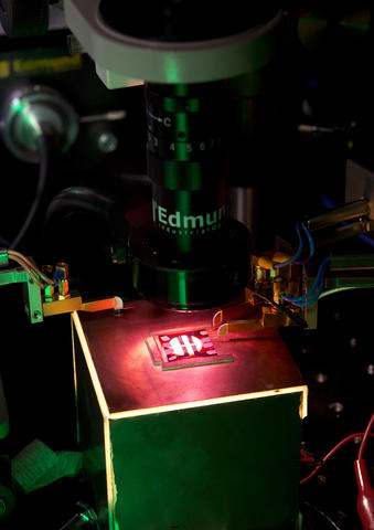
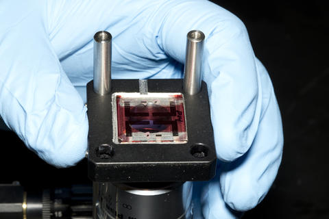
Organic photovoltaic sample under test.
Photovoltaic devices, also known as solar cells, produce electrical power when exposed to light, and that technology has enabled a fast-growing industry. The most familiar designs use rigid layers of silicon crystal. But recently, intense interest has focused on organic photovoltaic (OP) devices which use inexpensive organic semiconductor materials sandwiched between two metal electrodes. OP devices can be made flexible and easily portable. Imagine a tent that, once set up, acts as a large solar system that can be used to recharge portable electronics and lights for the upcoming night of camping.
However, at this time organic photovoltaic devices are hindered by low efficiency relative to commercial solar cells – in part because quantifying their electrical properties has proven challenging. Therefore, predictive models and quantitative metrics for device performance are critically needed.
Scientists from NIST's Physical Measurement Laboratory, led by the Semiconductor and Dimensional Metrology Division's David Gundlach and Curt Richter, along with James Basham, a guest researcher from Penn State University, have developed a method that allows the prediction of the current density-voltage curve of a photovoltaic device.1 This new method uses a common measurement technique (impedance spectroscopy) that is affordable, widely available to manufacturers, and relatively easy to perform. The technique is repeatable, non-destructive, reasonably fast (≈15 min to test a device), and—thanks to a rigorous analysis and methodology created by Basham—provides a comprehensive readout of the device's current-voltage properties that was previously illusive to most researchers working in the field. Finally, this technique allows the device to be tested in real-world conditions.
"This measurement breakthrough should allow us to more rapidly optimize solar cells," Richter states. "We're able to look at what happens electronically throughout the entire device. Importantly, how long does the charge exist once created and how long does it take to get the photogenerated charge through the semiconductor mixture to the electrodes? The larger the difference between the charge lifetime and device transit time greatly improves the likelihood that a photovoltaic device will be a more efficient source of electrical power."
Currently at the laboratory level, current-voltage testing of organic photovoltaic devices is typically done by analyzing device operation at either extreme of the device's bias spectrum—that is, a short circuit or an open circuit—and trying to infer from those results what is happening electrically within the device. But, when the device does not perform as a "textbook" or "ideal" solar cell then the picture of what's going on in the device between these bias extremes quickly becomes clouded.
"That approach only works if the recombination (where the charge carriers are eliminated rather than continuing to flow through the device) at one bias is nominally identical to the charge generation at the other," Gundlach says. "In a good device, those should be about equal. In a non-ideal device, they could be vastly different. With our technique, we can actually map the full range of the characteristics from one extreme to the other and disentangle generation, transport, and different loss mechanisms throughout the entire bias range."
The output of this new technique is the precise reproduction of the device's current density-voltage curve through the entire voltage range between the bias extremes. This allows researchers to pinpoint where problems exist in the device and can serve as a blueprint for what to fix in the device.
"Combining the physical properties, lifetimes, and carrier concentrations with an accurate nanoscale picture of the semiconductor film's microstructure really gives a complete picture of how the device operates and what limits these devices from reaching their theoretically predicted performance limits," Gundlach explains. "Our colleagues in the Materials Measurement Laboratory at NIST have greatly advanced the field's understanding of the latter. We are now in a much better position to put all of the pieces of information together, and then we can develop more physically accurate device models, better informed materials design guidelines, and ultimately more closely connect materials properties with processing methods and solar cell performance."
And since the physical process governing organic photovoltaics is very similar to other organic semiconductors (organic light-emitting diodes, for example, which are prevalent in electronic displays), future applications of this technique to other industries appear straightforward.
"A lot of the understanding being developed here can also be applied to make better organic light emitting diodes," Richter explains. The organic photovoltaic samples used in this study were developed in house at NIST. The 100 nm thick device has a three-layer structure—a top semi-transparent electrode, the organic photovoltaic, and a bottom electrode—placed on a 1 inch piece of glass.

The measurement itself is conceptually simple: "We're applying an oscillating voltage across the device and measuring the current that comes out," Richter explains. "We do this underneath the simulated sunlight. Mathematically, we're looking at the phase shifting of the current out relative to the voltage in."
These results, combined with Basham's analysis and methodology, provide a relatively inexpensive measurement that has tremendous value in understanding dominant loss mechanisms across the entire bias range of a device.
"Now, a small start-up company can go out and buy an impedance spectrometer and do this measurement with our paper in hand because it tells them how," Gundlach states.
"We can also do these same measurements absent the light source along the same voltage range," Gundlach continues, "and you don't get exactly the same answer. There are parts of the community that have argued that you can do these dark measurements and get the same answer."
More recently, Gundlach and Basham, in collaboration with NIST's Material Measurement Laboratory, used this technique in combination with separate measurement technique called Large Perturbation Transient Photovoltage (LPTP).2 In LPTP, the organic photovoltaic sample is illuminated with a laser pulse, which results in a temporary high-voltage that decays over a time from nanosecond to seconds. The voltage is measured, and a data curve is produced based on the time it takes for the voltage to drop back down to its dark state. These resulting data provide additional information about the recombination effects in the device that impedance spectroscopy is unable to provide.
Comparisons of the photogenerated charge lifetime as a function of charge density over a large range of charge density produced by both methods were the same, confirming that both techniques could sensitively and accurately measure generation and recombination processes in a consistent way.
"That's an important validation of these measurement techniques and analysis methods that has not been explicitly shown before for these devices; only assumed," Gundlach states.
1J. I. Basham, T. N. Jackson, D. J. Gundlach, "Predicting the J-V Curve in Organic Photovoltaics Using Impedance Spectroscopy," Advanced Energy Materials, Vol. 4, No. 9, 7 p., (02-Jun-2014)
2L. C. C. Elliott, J. I. Basham, K. P. Pernstich, P. R. Shrestha, L. J. Richter, D. M. DeLongchamp, D. J. Gundlach, "Probing Charge Recombination Dynamics in Organic Photovoltaic Devices under Open-Circuit Conditions," Advanced Energy Materials, 8 p. (12-Jun-2014)

