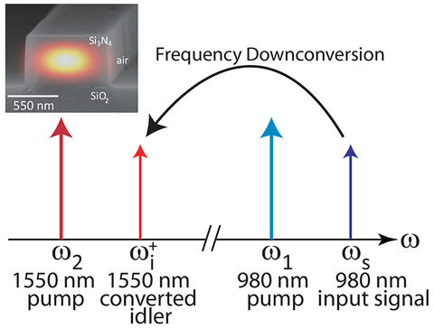
Using nanofabricated waveguides in a silicon-based platform, researchers from the NIST Center for Nanoscale Science and Technology (CNST) have developed a frequency conversion interface between the optical transition wavelengths in quantum dots and in naturally occurring atoms and the telecommunications wavelength band.* Optical frequency conversion is an important resource for applications in both classical and quantum information processing, where it can link components of a system that perform optimally at their specific tasks, but operate at different wavelengths.
In this work, the researchers focused on an interface between near-infrared wavelengths below 1000 nm, where systems like semiconductor quantum dots and neutral alkali atoms have their optical transitions, and the telecommunications band of 1550 nm, which is the lowest loss wavelength through which light propagates in an optical fiber. To develop this interface, they built upon previous work in which they demonstrated that a low-noise frequency conversion process called four-wave-mixing Bragg scattering could be realized in silicon nitride waveguides fabricated on a silicon substrate. While that work focused on demonstrating conversion over a range of a few nanometers with conversion efficiencies reaching a few percent, here the authors extended the conversion range to nearly 600 nm. This improvement was made possible by the nature of the four-wave-mixing process, in which the locations of the two pump fields, input signal, and converted signal can be re-arranged while preserving the requirements of energy and momentum conservation.
The authors demonstrated that the process was bi-directional (signals can be converted from 980 nm to 1550 nm and back), and developed designs to interface light at wavelengths all the way down to 637 nm — characteristic of the nitrogen vacancy center in diamond — with the 1550 nm band.
Future work will be focused on significantly increasing the conversion efficiency levels of these devices by optimizing the geometries and using resonant cavities.
The NIST Center for Nanoscale Science and Technology (CNST) is a national nanotechnology user facility that enables innovation by providing rapid access to the tools needed to make and measure nanostructures. Researchers interested in accessing the techniques described here or in collaborating on their future development should contact Kartik Srinivasan.
*A chip-scale, telecommunications-band frequency conversion interface for quantum emitters, I. Agha, S. Ates, M. Davanço, and K. Srinivasan, Optics Express 21, 21628–21638 (2013).
NIST Publication Database Journal Web Site

