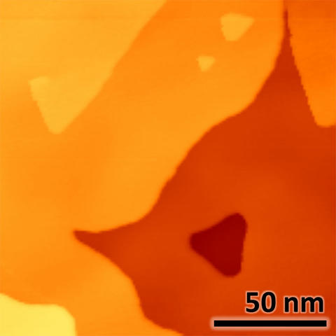
Researchers from the NIST Center for Nanoscale Science and Technology (CNST), the University of Maryland, and Seoul National University, Korea have achieved electric-field control of the energy levels at the surface of two potentially important materials, bismuth selenide (Bi2Se3) [1] and antimony telluride (Sb2Te3) [2]. These materials are topological insulators, which are hybrid materials that are electrical insulators in their interiors but are exotic, graphene-like conductors at their surfaces.
Understanding how to use electric fields to control the energy levels at the surfaces of such topological insulators could make these materials extremely promising for a variety of electronic applications. This type of electric field control mirrors the gating used to turn on and off the field effect transistors found in countless everyday electronic devices. Achieving this control while characterizing the material's surface directly with scanning tunneling microscopy—in principle an ideal method to observe the effects of electric fields—has been particularly challenging, because the typical processing needed to create the required electrodes damages the surface to be studied. The CNST researchers and their collaborators have overcome this challenge by developing high temperature sample holders that contain both the gating electrode and a dielectric upon which topological insulator films can be grown in-situ using molecular-beam epitaxy. The specially fabricated samples holders, made in the CNST NanoFab, incorporate strontium titanate substrates with pre-patterned electrodes, allowing pristine films to be deposited after the electrode fabrication process [1].
Using the gating electrode to apply an electric field, the researchers are able to tune the doping of the top surfaces of the Bi2Se3 and Sb2Te3 topological insulator devices in order to vary their surface energy levels. In a particularly noteworthy result, the gating measurements indicate that for ultra-thin Sb2Te3 it may be possible to reversibly change the material from an ordinary insulator to a topological insulator and thereby switch "on and off" special properties that can exist at the thin film boundaries that may be useful in electrical device applications.
[1] Scanning tunneling microscopy of gate tunable topological insulator Bi2Se3 thin films, T. Zhang, N. Levy, J. Ha, Y. Kuk, and J. A. Stroscio, Physical Review B 87, 115410 (2013).
NIST Publication Database Journal Web Site
[2] Electric field tuning of the surface band structure of topological insulator Sb2Te3 thin films, T. Zhang, J. Ha, N. Levy, Y. Kuk, and J. Stroscio, Physical Review Letters 111, 056803 (2013).
NIST Publication Database Journal Web Site

