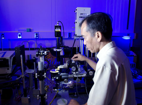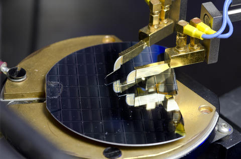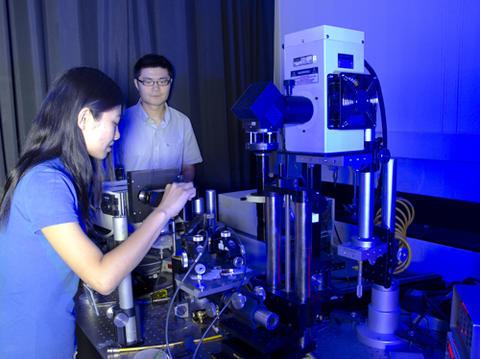
Nhan Nguyen demonstrates how he performs optical measurements on a graphene-insulator-semiconductor sample structure.
That graphene is the hot new material in the world of future electronics manufacturing is well known. With its high carrier mobility and low noise, graphene is seen as a possible candidate to ultimately replace silicon in integrated circuits. Finding a way to fully characterize new materials such as graphene is critical to the ultimate goal of successful engineering and manufacturing of next-generation devices. Researchers at NIST's Physical Measurement Laboratory have brought us one important step closer to this goal with the determination of graphene's work function and the band alignment of a graphene-insulator-semiconductor structure by using the combined optical techniques of internal photoemission (IPE) and spectroscopic ellipsometry (SE).

"We are the only group in the U.S. who use the techniques full time," explains Nhan Nguyen, of the PML's Semiconductor and Dimensional Metrology Division. Nguyen, a world-renowned expert in both IPE and SE, brings a wealth of experience to the state-of-the-art facilities at NIST. "Nhan is one of, arguably, two photoemission specialists world-wide that have a tremendous depth and experience in that measurement technique," states David Gundlach, Nguyen's Project Leader. "As far as ellipsometry, there are relatively few ellipsometric specialists that have the spectral range that he can cover with the measurement apparatuses that he has available to him at NIST."
Nguyen originally used the combined measurement techniques to determine successfully the energy barrier heights and band structure of metal-oxide-semiconductor (MOS) devices. Building on that study, his hope was that he could characterize a graphene-insulator-semiconductor (GIS) device in a similarly non-destructive manner. Current methods for characterizing such a device employ destructive techniques for cross sectioning and analyzing. These methods not only destroy the device, but also potentially compromise the very electronic properties that are being measured.
Band alignment is important in GIS devices because the correct band offsets are necessary to prevent undesirable leakage currents in device applications. In other words, if the layers are not lined up in a precise way, the device will behave differently than anticipated, perhaps even failing entirely. This information is critical for the successful engineering and reproducible manufacturability and reliability of such devices. Yet, until now, no detailed study on the band alignment of these devices had been reported.

Using a combination of IPE (setup included a 150 W broadband Xenon light source and a quarter-meter Czerny Turner monochromator to tune the incident light with photon energy) and SE, Nguyen was able to view the whole picture of the structure's band alignment. IPE revealed the offset between bands and how they aligned with respect to each other, but only on one side of the device. SE measurements allowed the calculation of the band gaps, which led to the determination of the entire band structure. "In devices," Nguyen explains, "we want band offsets large enough so that you don't have noise or leakage. If they are too close, the electrons can jump across. With IPE, you can really look deeper below the surface of the material without changing the properties of the interface."

The potential impact of this completed study and published results* on the development of future devices is substantial. Instead of developing a device and destructively measuring what was built afterwards to determine its electrical properties, devices can be engineered with known electrical behavior from the start. "Nhan's technique is extremely valuable in advancing future electronics in the fronts of semiconductor electronics, advanced manufacturing, and nano manufacturing," Gundlach concludes.
In addition to studying the manipulation of energy levels in a graphene layer, future studies will utilize graphene's unique properties to study other materials. Since graphene can be applied in a very thin and continuous layer, it allows for much better optical transmission than the semi-transparent metals previously used. Nguyen intends to stack the graphene layer onto other layers with unknown properties, using the graphene as a key to understanding the unknown layers beneath. "This has given us access to measurements that were previously unavailable," Nguyen states. This is critical as the industry moves beyond CMOS technology. New semiconductor materials used in more complicated device structures and architectures need to be characterized. And now Nguyen and colleagues have demonstrated a non-destructive way to do it.
-- reported, written, and photographed by Erik Secula
-- animation by Aakash Patel
*R. Yan, Q. Zhang, W. Li, I. G. Calizo, T. Shen, C. A. Richter, A. R. Hight Walker, X. X. Liang, A. Seabaugh, D. Jena, H. G. Xing, D. J. Gundlach, N. V. Nguyen, "Determination of Graphene Work Function and Graphene-Insulator-Semiconductor Band Alignment by Internal Photoemission Spectroscopy," Applied Physics Letters, 101, 022105 (2012)

