
Official websites use .gov
A .gov website belongs to an official government organization in the United States.
Secure .gov websites use HTTPS
A lock (
) or https:// means you’ve safely connected to the .gov website. Share sensitive information only on official, secure websites.
Local screening is an issue because vibrational modes lie at very small energies – below about 200 meV. In microscopy, keV electrons produce stron electronic response at higher energies which can screen the incident electron potential, suppressing the electron’s ability to produce interactions at long range. Thus in these materials, even bulk phonon scattering can contain high spatial resolution components that can be mapped.
For the very low energy bulk vibrational modes, the occupied state population at room temperature strongly distorts the experimental scattering at and below 30-50 meV energies, especially for the acoustic modes. Scattering intensities below 25-30 meV become very strong, as much as 10% of the zero loss peak. While these increase the visibility of the vibrational modes near the zero loss, the distortion clearly needs to be removed to reveal the density of states for comparison with other spectroscopies.
Finally, simple optical modeling of electron scattering fails for several symmetries of phonon modes in typical materials. Transverse optical, and acoustic modes do not appear in the IR spectroscopies, for instance. It is becoming clearer that details driven by spatial resolution, and inclusion of multipole scattering components are important to a full understanding of the experimental results [6-7].
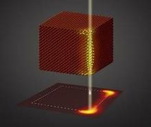
This research was supported by the US Department of Energy, Basic Energy Sciences (#DE-SC0005132). The author also acknowledges collaboration with M.J. Lagos, A. Trügler, and U. Hohenester. The accompanying graphic is the work of Trügler.
Philip E. Batson
Department of Materials, Science and Engineering / Department of Physics / IAMDN / Rutgers University, USA