An official website of the United States government
Here’s how you know
Official websites use .gov
A .gov website belongs to an official government organization in the United States.
Secure .gov websites use HTTPS
A lock (
) or https:// means you’ve safely connected to the .gov website. Share sensitive information only on official, secure websites.
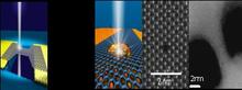
From left to right: illustrations of nanoribbon sculpting with the electron beam; passage of a DNA molecule through a nanopore; illustration of nanopore drilling with an electron beam inside of the TEM; one-atom-large nanopore in a MoS2 sheet; armchair phosphorene nanoribbon sculpted in the AC-TEM.
Electron beams constitute powerful tools to shape materials with atomic resolution inside a transmission electron microscope (TEM). I will describe experiments where we push the limits of device size to atomic scale in 2D materials beyond graphene (MoS2, WS2, MoTe2, black phosphorous) and expand their function and precision, while addressing fundamental questions about structure and properties at nanometer and atomic scales. Experiments are performed in situ and ex situ TEM. In situ TEM experiments include fabrication of nanoribbons and field-effect-transistors from novel two-dimensional materials down to sub-nm widths. Ex situ TEM experiments include the ultrafast, all-electronic detection and analysis of biomolecules by driving them through tiny holes – or nanopores – in thin membranes, including the efforts towards mapping a human genome under 10 min. As molecules are driven through nanopores in solution, they block the ion current flow resulting in current reductions from which molecule’s physical and chemical properties are inferred. DNA, proteins, microRNA and other biomolecules can be analyzed. The temporal, spatial resolution and sensitivity in these experiments have been improved over the last few years thanks to advanced materials, device designs and new electronics.