
Official websites use .gov
A .gov website belongs to an official government organization in the United States.
Secure .gov websites use HTTPS
A lock (
) or https:// means you’ve safely connected to the .gov website. Share sensitive information only on official, secure websites.
Kelvin Probe Force Microscopy: Developments and Applications
Summary
Kelvin probe force microscopy (KPFM) is an atomic force microscopy (AFM) mode in which the contact potential difference (CPD) between a conductive AFM probe and a sample is extracted by observing the electrostatic interaction between probe and sample at the nanoscale level. In addition to that, KPFM became one of the most used AFM imaging modes for electric surface property characterization through the plethora of probe-sample interactions that are either directly or indirectly extracted from CPD measurements across a large variety of materials and structures including metals, semiconductors, dielectrics, photovoltaics, polymers, ferroelectrics, and biological samples. In our lab we use commercially implemented KPFM methods to study materials and device structures for various nanoscale applications. We also develop high-speed digitization open-loop KPFM variants for a more inclusive and detailed measurement of electrical interactions.
Description
The most common versions of KPFM are in the forms of amplitude-modulation KPFM (AM-KPFM) and frequency-modulation KPFM (FM-KPFM). These modes are routinely implemented on commercial AFMs as closed-loop (CL) procedures, seeking to determine the local CPD between an AFM probe and the investigated sample by nullifying either the electrostatic force (CL AM-KPFM) or the gradient of the electrostatic force (CL FM-KPFM) between the probe and sample. The characteristic CL KPFM drive includes a combination of DC and AC voltages, usually with the first harmonic or sidebands around the first harmonic targeted by the feedback nullification to extract the tip-sample CPD. In addition to CL KPFM variants, various open-loop (OL) KPFM implementations were developed to mitigate artifacts associated with the CL bias feedback, measure voltage sensitive materials, and enable the observation of fast electrodynamic processes. Examples of OL KPFM include dual harmonic KPFM (with measurement of the first two harmonic amplitudes) and methods with high-speed digitization of the response under an AC bias drive. We developed a new OP KPFM operating in a single-pass PeakForce Tapping mode that can provide both mechanical (from the in-contact parts of the taps) and surface potential (from the out-of-contact part of the taps) measurements at every pixel of the scan.
Major Accomplishments
KPFM for studying advanced 2D/3D semiconductor heterostructures
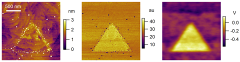
We used KPFM in tandem with other local spectroscopies to study the seamless integration of molybdenum disulfide (MoS2) epitaxial layers on gallium nitride (GaN) substrates as prototypes for electronic devices based on 2D/3D vertical heterostructures. The surface potential measurements provided by KPFM complemented other AFM-based characterizations (topography, adhesion, and electrical current) to detail the morphology and vertical charge transport in 2D/3D fabricated structures.
KPFM for studying the controlled doping of 2D layered materials by surface charge transfer
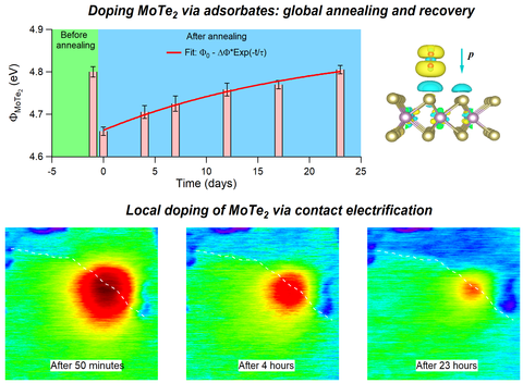
We used KPFM to study the inducing and tuning of the p-doping of MoTe2 layers through the controlled of surface adsorbates, both globally (via thermal annealing) and locally (via contact electrification). Our results demonstrated controlled p-type doping of MoTe2 by physisorbed oxygen on stoichiometric surfaces (with no vacancies), in contrast to more commonly attributed n-type doping on MoTe2 to Te vacancies, and the switch to p-type doping by H2O/O2 redox couple occurring in air. We also illustrated local control of the surface charge doping by contact electrification using the probe of an electrostatic force microscope as a floating gate. After annealing or contact electrification, the air-exposed MoTe2 surfaces exhibit a slow reversal processes of readsorption of oxygen, with the restore of the p-type doping. These investigations can complement typical field effect transistor measurements used to extract electronic transport properties of devices based on 2D materials. As a reversible and controllable nanoscale physisorption process, surface charge transfer doping can thus open new avenues for the emerging field of 2D-based electronics.
High-speed digitization of open-loop KPFM
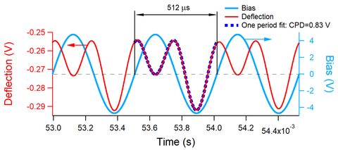
Closed-loop (CL) KPFM configurations are routinely implemented on commercial AFM instruments. Few open-loop (OL) AM KPFM were proposed as a viable alternative for reducing the feedback-loop effects associated to CL operation. However, OL FM-KPFM remained largely unexplored. The net advantage of FM-KPFM variants over those of AM-KPFM is their enhanced local sensitivity in CPD measurements due to the screening effect of the force-gradient on the cantilever stray capacitive couplings. We developed an OL sideband FM-KPFM in which both the amplitude and frequency can be tracked and used to extract CPD. This is done through either the parabolic or time series analysis of the high-speed digitized signals. Although OL modes come with issues of storage and processing of large data sets, the great promise of these type of measurements is on a more inclusive measurement and description of the electrostatic probe-sample interaction that can enable complementary characterization of the sample properties.
Open-loop KPFM in single pass PeakForce Tapping
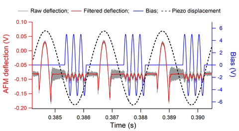
We developed an OL AM-KPFM method in the single-pass scanning of the PFT mode. A sinusoidal bias modulation was synchronized with the out-of-contact intervals of the PFT motion to perform OL AM-KPFM measurements at each location in the scan. The high-speed digitization of the piezo displacement, AFM deflection, and applied bias signals provided detailed observation of the tip–sample mechanical and electrical interactions for topography reconstruction and KPFM characterization. The advantage of using OL AM-KPFM resides in the direct and easy implementation of the measurements with the possibility of accommodating relevant descriptions of the electrostatic interactions probed over various regions of a sample.
Relevant Publications
- Surface potential by KPFM in 2D/3D semiconductor heterostructures, ACS Nano 10, 3580−3588 (2016); https://pubs.acs.org/doi/10.1021/acsnano.5b08008
- Doping 2D layered materials by surface charge transfer, ACS Appl. Mater. Interfaces 12, 18182−18193 (2020); https://pubs.acs.org/doi/10.1021/acsami.0c04339
- High-speed digitization of open-loop KPFM, Nanotechnology 31, 385706 (2020); https://iopscience.iop.org/article/10.1088/1361-6528/ab9af0
- Open-loop KPFM in single pass PeakForce Tapping, Beilstein J. Nanotechnol. 12, 1115–1126 (2022); https://www.beilstein-journals.org/bjnano/articles/12/83
Impact and customers
- Develop instrumentation, measurement protocols, and calibration procedures for various KPFM-based methods. Implement KPFM methodology into existing AFM platforms.
- Perform state-of-the-art quantitative surface potential and related KPFM measurements on samples and devices used in advanced nanoscale applications.
- Collaborations with and knowledge dissemination to KPFM developers on nanoscale surface potential measurements and analysis.
Contacts
-
(301) 975-3675