
Official websites use .gov
A .gov website belongs to an official government organization in the United States.
Secure .gov websites use HTTPS
A lock (
) or https:// means you’ve safely connected to the .gov website. Share sensitive information only on official, secure websites.
AFM-based Nanomechanical Tests and Characterizations
Summary
The AFM probes themselves can be used in various setups to manipulate and probe specimens in bending, fracture, and other nanoscale mechanical tests.
Major Accomplishments
Nanoscale bending tests by AFM manipulation. A sequential AFM manipulation-scanning protocol was developed to bend nanowires (NWs) simply held by adhesion on a flat substrate. The adhesion between the NWs and substrate provided strong-enough forces to maintain the NWs in the imposed bending states. In various bending configurations (hook and loop), it was possible to observe large bending stress states of Si NWs as their radius of curvature was progressively reduced. The bending states prior to failure were analyzed in detail to measure the bending dynamics and the ultimate fracture strength of the investigated nanowires. The benefit of the method is that it does not require special grips at the ends of the NW tested and allows a post-observation of the bending states.
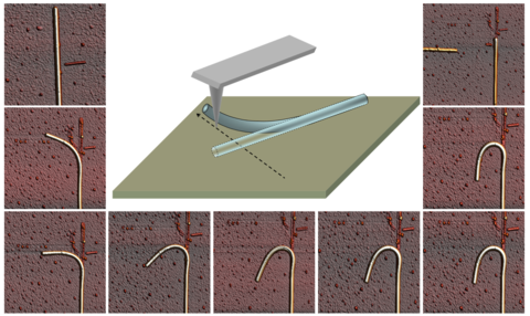
Figure 1: By using an AFM probe as a nanoscale manipulator, a Si NW was progressively bent from a straight state (top left) to fracture (right top). The intermediate bending states were imaged in regular AFM scans (counterclockwise from top left to top right) to detail the accommodated stress during bending and capture the maximum bending strength of the nanowire prior to its fracture.
Nanoscale buckling of high-aspect-ratio organosilicate fins during hard-mask patterning. A hybrid characterization method was implemented to analyze quantitatively the buckling of organosilicate fins that are capped with hard masks of TiN in the process of lithographic formation of Cu/low-k dielectric circuits. Based on measurements of mechanical properties and geometric dimensions, the states of fins with various degrees of buckling were accurately described and used to put together a framework for guiding the design of future nanoscale interconnect architectures.
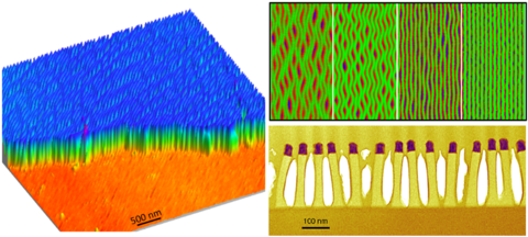
Figure 2: Left: AFM view of the top and sides of buckled fins. Top right: AFM maps of the top of the buckled fins in states of various degrees of buckling amplitude and wavelength. Bottom right: TEM image of the cross-section of buckled TiN-capped fins.
Nanoparticle size metrology. Inherently, the synthesized nanoparticles have a large size distribution that can adversely affect their use and performance in various applications in the fields of medicine, biology, and material science. We use AFM to accurately measure the size distribution of various nanoparticles (e.g. Au, silica, Zn, Cu, PEGylated metallic particles etc.) simply supported on flat substrates (e.g. fresh cleaved mica).
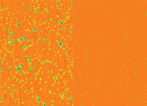
Figure 3: AFM images of silica nanoparticle separation based on size-dependent aggregation induced by the critical Casimir effect: Before (left) and after (right) separation.
Relevant Publications
- Bending strength of nanowires by AFM: Nano Letters 12, 2599 (2012); https://pubs.acs.org/doi/abs/10.1021/nl300957a
- Bending and fracture of nanowires by AFM: Journal of Materials Research 27, 562 (2012); https://doi.org/10.1557/jmr.2011.354
- Buckling of organosilicate fins during patterning: Nano Letters 15, 3845 (2015); https://doi.org/10.1021/acs.nanolett.5b00685
- Nanoparticle size-measurement by AFM: International Journal of Medicine 11, 1567 (2016); https://doi.org/10.2147/IJN.S101463
- Nanoparticle size-measurement by AFM: PLOS one 12, e0189273 (2017); https://doi.org/10.1371/journal.pone.0189273
- Nanoparticle size-measurement by AFM: Soft Matter 14, 1311 (2018); https://doi.org/10.1039/C7SM01971H
Contacts
-
(301) 975-3675