
Official websites use .gov
A .gov website belongs to an official government organization in the United States.
Secure .gov websites use HTTPS
A lock (
) or https:// means you’ve safely connected to the .gov website. Share sensitive information only on official, secure websites.
NanoFab Tool: Zeiss Gemini 560 Field Emission Scanning Electron Microscope
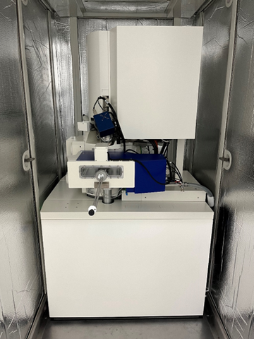
Photograph of Zeiss Gemini 560 Field Emission Scanning Electron Microscope.
The Zeiss Gemini 560 Field Emission Scanning Electron Microscope (FE-SEM) is a high resolution FE-SEM which provides nanoscale imaging from 100 mm diameter wafers down to small pieces. It has superb resolution and image quality at high and low accelerating voltages. The Gemini 560 has a high efficiency Inlens secondary detector for high contrast, ultra-high resolution surface imaging and Everhart Thornley secondary electron detector for 3-dimensional topographic imaging.
Specifications/Capabilities
- Digital system with full function computer control.
- Resolution: 0.5 nm at 15 kV; 0.8 nm at 1 kV, 1.0 nm at 500 V.
- Accelerating Voltage: 0.02 – 30.0 kV
- Magnification: 50 times to 2,000,000 times.
- High efficiency Inlens secondary detector for ultra-high resolution surface information.
- Motorized stage with travel in 6 axes.
- Integrated 100 mm airlock.
- Small pieces supported: Yes.
Usage Information
Supported Sample Sizes
- Maximum wafer diameter: 100 mm.
- Small pieces supported: Yes.
Typical Applications
- Optical waveguides.
- Silicon gate devices.
- Solar cell fabrication.