
Official websites use .gov
A .gov website belongs to an official government organization in the United States.
Secure .gov websites use HTTPS
A lock (
) or https:// means you’ve safely connected to the .gov website. Share sensitive information only on official, secure websites.
NanoFab Tool: ThermoFisher Hydra PFIB Dual Beam Scanning Electron Microscope (SEM) and Focused Ion Beam (FIB)
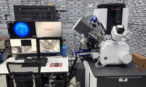
The ThermoFisher Helios 5 Hydra PFIB dual-beam microscope combines a monochromated field emission scanning electron microscope (FE-SEM) with an advanced plasma focused ion beam (PFIB) column for fast, precise nanomachining and nanoscale structural characterization. Enhanced capabilities include simultaneous chemical characterization using energy dispersive x-ray spectroscopy (EDS) and time-of-flight secondary ion mass spectrometry (TOF-SIMS) as well as material crystallographic characterization using electron backscatter diffraction (EBSD). The tool supports a variety of substrates ranging from 150 mm diameter wafers down to small pieces.
Specifications/Capabilities
- FE-SEM
- Resolution: sub-nanometer from 1 kV to 30 kV.
- High resolution in-lens electron detectors with Through Lens (TLD, secondary and backscatter mode), In Column (ICD, low-loss backscatter) detectors.
- Scanning transmission electron microscopy (STEM) detector with bright-field (BF), dark-field (DF), and high-angle annular dark-field (HAADF) segments.
- Retractable dedicated backscatter detector with annular segments (ABS/CBS).
- Electron beam deceleration for 50 V effective landing voltage.
- 5-axis stage with 150 mm X-Y range and full rotation.
- Integrated plasma cleaner to minimize contamination.
- FIB (Plasma ion source)
- Selectable gas species (Xe, Ar, Oxygen, Nitrogen), automated fast switching
- High current for fast milling of large areas.
- High efficiency secondary ion detector.
- Electron flood gun for ion charge compensation.
- Secondary Ion imaging detector (ICE).
- Integrated beam current measurement for automatic milling/deposition recipe correction and consistent results.
- Real time monitoring of milling and deposition processes.
- End point monitoring for cross sectioning and circuit edit applications.
- Easy Lift manipulator for removing transmission electron microscopy (TEM) and atom probe tomography (APT) samples.
- Enhanced capabilities for simultaneous materials characterization
- Energy dispersive x-ray spectroscopy Oxford Instruments Ultim Max 100 mm2 SDD-EDS detector (element characterization).
- Electron backscatter diffraction Oxford Instruments Symmetry 3 EBSD detector (crystallographic characterization).
- Time-of-Flight Secondary Ion Mass Spectrometry using TOFWerk fibTOF detector (elemental and isotopic 3D imaging).
- Deben Enhanced Coolstage -25°C to +160°C for high vacuum heating and cooling applications (small samples only).
- Gas injection system chemistries
- Tungsten deposition.
- Platinum deposition.
- Carbon deposition.
- Insulator deposition using tetraethyl orthosilicate (TEOS).
- Selective carbon etch.
- Insulator enhanced etching using xenon difluoride (XeF2).
- Software packages
- MAPS – Automated large area imaging and stitching, correlative
- Auto TEM – Automated TEM sample preparation including liftout.
- TOF Explorer – acquisition and analysis for Time-of-Flight mass spectrum, depth profiles, imaging overlay
- Auto Slice and View – Automated sequential milling and image capturing generates datasets for 3D reconstruction.
- EDS3 – captures EDS data during sequential milling.
- EBS3 – captures EBSD data during sequential milling.
- Aztec – User-friendly EDS/EBSD data collection and analysis software now with Live SEM capability.
- Automated Rocking Polish to minimize FIB-induced artifacts.
- Automated Spin Mill for large planar milling and imaging.
- NanoBuilder – Advanced computer aided design (CAD) based patterning using GDSII files.
- NEXS – CAD based navigation for chip-level orientation facilitating fault isolation, failure analysis, sample preparation and circuit edit.
Usage Information
Supported Sample Sizes
- Maximum wafer diameter: 150 mm.
- Holders for 100 mm, 125 mm, and 150 mm diameter wafers.
- Small pieces supported: Yes.
- Non-magnetic materials: Yes.
- Biological materials: No.
- Radioactive materials: No.
Typical Applications
- Nanometer scale patterning.
- 3D tomography.
- Materials characterization.
- Prototyping of nanoscale devices.
- Preparation of TEM lamellae.
- Sample preparation for atom probe tomography.
- Failure analysis.
- Circuit editing.
- Analysis and mapping of material and chemical sample composition.
- Mapping of crystal orientation.
- Phase identification.
- Collection of grain boundary and localized strain data.