
Official websites use .gov
A .gov website belongs to an official government organization in the United States.
Secure .gov websites use HTTPS
A lock (
) or https:// means you’ve safely connected to the .gov website. Share sensitive information only on official, secure websites.
NanoFab Tool: Sandvik LPCVD Amorphous and Polycrystalline Silicon
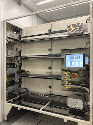
Photo of the Sandvik anneal furnaces
The Sandvik low pressure chemical vapor deposition (LPCVD) polysilicon furnaces supports amorphous and polycrystalline silicon deposition in the NanoFab. The furnace stack allows the deposition of n typed doped (phosphine) and undoped polysilicon films on substrates ranging from small chips to wafer diameters up to 150 mm. All samples require SC1 and SC2 cleans prior to processing.
Specifications/Capabilities
- Automatic recipe controller using Variable Parameter Table (VPT)
- Maximum Temperature: 650 °C.
- Maximum Deposition Thickness: 2 µm.
- Standard processes:
- Undoped polysilicon
- Doped (phosphine) polysilicon
- Wafer diameters: 75 mm (3 in), 100 mm (4 in), and 150 mm (6 in)
- Small pieces supported: Yes
Typical Applications
- Conducting layer (doped)
- Piezo resistive gauges and thermocouples
- Gate Transistor
- Insulating layer (undoped)
- High purity mask
- Fabry-Perot interferometer