
Official websites use .gov
A .gov website belongs to an official government organization in the United States.
Secure .gov websites use HTTPS
A lock (
) or https:// means you’ve safely connected to the .gov website. Share sensitive information only on official, secure websites.
NanoFab Tool: Oxford PlasmaPro 100 Inductively Coupled Plasma (ICP) Dielectric Etcher
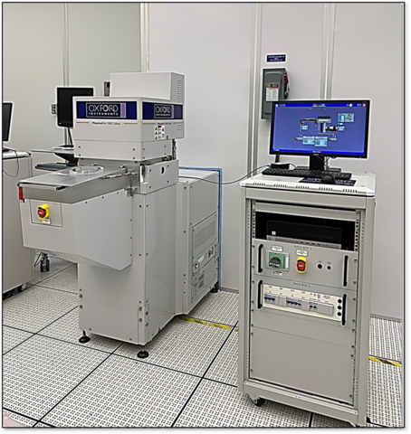
Photograph of the Oxford PlasmaPro 100 Inductively Coupled Plasma (ICP) Dielectric Etcher.
The Oxford PlasmaPro100 ICP dielectric etcher is a system that allows anisotropic etching of silicon oxide and silicon nitride. The tool is equipped with multiple etch gases and a temperature-controlled electrode. The manual wafer load system can accommodate substrates ranging from 200 mm diameter wafers down to small pieces.
Specifications/Capabilities
- The Cobra ICP etch sources produce a high density of reactive species at low pressure.
- Full area process gas inlet showerhead for uniform gas distribution.
- Electrode temperature range: -150 °C to +400 °C.
- Wafer clamping with Helium backside cooling.
- Process Gases: Ar, He, N2, O2, H2, CHF3, CF4, C4F8, C2F6 and SF6
- Controlled profile etching.
- Wafer diameters: 75 mm, 100 mm (default), 150 mm, and 200 mm.
- Small pieces supported: Yes.
Typical Applications
- SiO2 and Si3N4 based device fabrication.