
Official websites use .gov
A .gov website belongs to an official government organization in the United States.
Secure .gov websites use HTTPS
A lock (
) or https:// means you’ve safely connected to the .gov website. Share sensitive information only on official, secure websites.
NanoFab Tool: Oxford PlasmaPro 100 Inductively Coupled Plasma (ICP) III-V Etcher
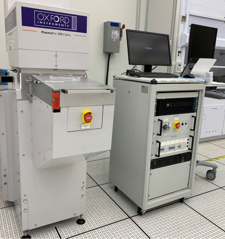
The Oxford PlasmaPro100 ICP etcher is configured for etching of III-V group semiconductors (InP and GaAs) using a chlorine gas-based plasma etch chemistry. The tool is equipped with 12 etch gases and a temperature-controlled electrode. The process flexibility allows users to expand the process control window and tailor etch feature profiles. The manual wafer load system can accommodate substrates ranging from 200 mm diameter wafers down to small pieces.
Specifications/Capabilities
- The Cobra ICP etch sources produce a high density of reactive species at low pressure.
- Solid state RF generators and close coupled matching network for fast and consistent etching.
- Full area process gas inlet showerhead for uniform gas distribution.
- Electrode temperature range: -150 ºC to +400 ºC.
- Wafer clamping with Helium backside cooling is available.
- Process Gases: Ar, He, N2, O2, CF4, SF6, Cl2, BCl3, SiCl4, CH4, H2 and HBr
- Controlled profile etching.
- Wafer diameters: 75 mm, 100 mm (default), 150 mm, and 200 mm.
- Small pieces supported: Yes.
Typical Applications
- III-V materials-based device fabrication.