
Official websites use .gov
A .gov website belongs to an official government organization in the United States.
Secure .gov websites use HTTPS
A lock (
) or https:// means you’ve safely connected to the .gov website. Share sensitive information only on official, secure websites.
NanoFab Tool: IPEC 472, Chemical Mechanical Polisher (CMP)
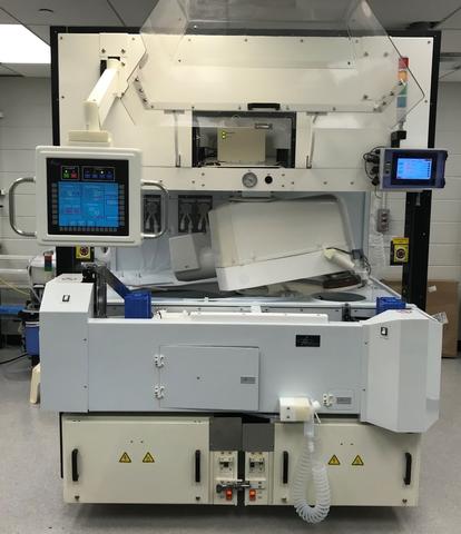
Photo of the Chemical Mechanical Polisher
The CMP removes material both chemically, by use of a corrosive colloidal slurry, and mechanically, by way of a wafer carrier under controlled pressure rotating against a rotating polishing pad, with carrier and pad having nonconcentric axes of rotation. It is equipped with a primary platen to remove the material and a secondary platen to do the final polish and minimize the surface roughness. The system removes irregular topography and leaves wafers planar with sub-nanometer roughness.
Specifications/Capabilities
- Sample size: 100 mm diameter wafers only (pieces are not allowed)
- Cassette-to-cassette capability, 25-wafer capacity
- Laterally oscillating wafer carrier
- In-situ pad conditioning on primary platen
- Within wafer non-uniformity: typically, less than 3 % sigma/mean
- Wafer-to-wafer non-uniformity: typically, less than 5 %
- The removal rate is dependent on material, rotation speeds, pressure, type of slurry, concentration and slurry flow rate and can vary from a few nm/min to several hundred nm/min.
Usage Information
Operating Instructions
Typical Applications
- Planarization of metal interconnects and vias
- Planarization of inter-layer dielectrics: typically, SiO2
- General sample polishing to minimize surface roughness
- Available Recipes: Silicon dioxide, Silicon, Silicon nitride, Gold