
Official websites use .gov
A .gov website belongs to an official government organization in the United States.
Secure .gov websites use HTTPS
A lock (
) or https:// means you’ve safely connected to the .gov website. Share sensitive information only on official, secure websites.
NanoFab Tool: Gemstar Atomic Layer Deposition
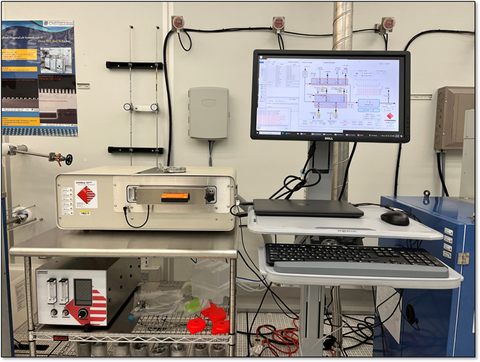
Photograph of the Arradiance Gemstar atomic layer deposition system.
The Arradiance Gemstar atomic layer deposition (ALD) system supports thermal ALD coating processes with precise ultrathin and pinhole free films in a compact benchtop platform. The system deposits films with thicknesses ranging from one atomic layer to several nanometers on a variety of substrate materials and can accommodate substrates ranging from small pieces to 200 mm diameter wafers. Standard processes include Titanium Oxide and Hafnium Oxide.
Specifications/Capabilities
- Precisely controlled ultrathin and pinhole free film coating.
- Film thicknesses ranging from one atomic layer to tens of nanometers.
- Maximum temperature: 200 °C.
- Standard deposition processes:
- Titanium Oxide.
- Hafnium Oxide.
Usage Information
Supported Sample Sizes
- Maximum wafer diameter: 200 mm.
- Small pieces supported: Yes.
Typical Applications
- Nanolaminates coatings.
- Nanostructure conformal coatings.
- High-aspect ratio feature coatings.