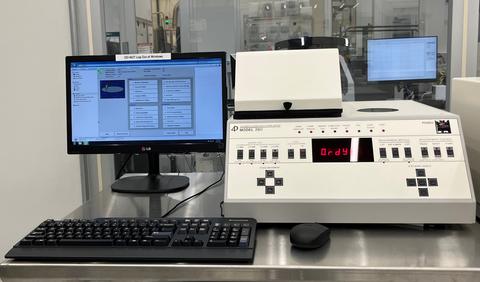
NanoFab Tool: Four Dimensions 280DI Sheet Resistance Mapping System

Four Dimensions 280DI Sheet Resistance Mapping System
The Four Dimensions 280DI sheet resistance mapping system uses the 4-point probe technique to measure the sheet resistance of substrates and films. The automated stage is capable of mapping up to 5,000 points per wafer and can handle substrates ranging from 200 mm down to small pieces. The wide resistance range and the choice of probe tips enable the mapping of a large variety of materials.
Specifications/Capabilities
- Resistance range: 1 mohm to 800 Gohm.
- Capacity: 1 wafer.
- Speed: 45 points per minute up to 800 kohm. Slower at higher ranges.
- Probe spacing: 1 mm.
- Probe force: 80 grams to 200 grams.
- Probe tip radius: 40 µm, 100 µm, and 200 µm.
- Front panel control for quick 1-point or 5-point measurements.
- Mapping capability
- Cartesian maps, up to 5,000 sites.
- Polar maps, up to 625 points.
- Diagonal maps.
- Software platform: Windows 7.
Usage Information
Supported Sample Sizes
- Maximum wafer diameter: 200 mm (8 in).
- Small pieces supported: Yes.
Typical Applications
- Thin film sheet resistance measurement.
- Bulk resistivity measurement.
- Thin film and resistivity uniformity.
Created January 30, 2015, Updated March 4, 2025

