
Official websites use .gov
A .gov website belongs to an official government organization in the United States.
Secure .gov websites use HTTPS
A lock (
) or https:// means you’ve safely connected to the .gov website. Share sensitive information only on official, secure websites.
NanoFab Tool: Filmetrics F40-UV Reflectometer
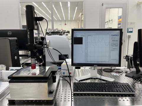
Filmetrics F40-UV Reflectometer
The Filmetrics F40-UV reflectometer provides users with rapid thin film thickness and optical constants measurements on most common device film stacks. The F40-UV combines a three objective microscope with an ultra-violet and visible light reflectance measurement system, allowing point specific film thickness and optical constants determination on substrates ranging from 200 mm diameter wafers down to small pieces.
Specifications/Capabilities
- Film thicknesses from several micrometers down to 4 nm.
- Index of refraction and absorption determination (n and k).
- Standard films:
- Oxide on silicon.
- Nitride on silicon.
- Polysilicon on oxide on silicon.
- Photoresist on silicon.
- Integrated video camera allows observation of the sample position
- Three microscope objectives: 15× for UV illumination; 5× and 50× for visible illumination
- Measurement spot sizes: 10 µm, 33 µm, 100 µm.
Usage Information
Supported Sample Sizes
- Maximum wafer diameter: 200 mm (8 in).
- Small pieces supported: Yes.
- Maximum thickness: 10 mm.
Typical Applications
- Thickness verification of deposited or etched films.
- Optical constants determination of deposited films.
- Process characterization of patterned substrates.