
Official websites use .gov
A .gov website belongs to an official government organization in the United States.
Secure .gov websites use HTTPS
A lock (
) or https:// means you’ve safely connected to the .gov website. Share sensitive information only on official, secure websites.
NanoFab Tool: FEI Helios NanoLab 660 Dual Beam Scanning Electron Microscope (SEM) and Focused Ion Beam (FIB) - FIB1
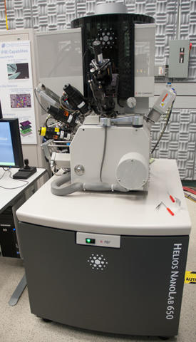
The FEI Helios 660 dual-beam microscope combines a monochromated field emission scanning electron microscope (FE-SEM) with an advanced focused ion beam (FIB) column for fast, precise nanomachining and nanoscale structural characterization. Enhanced capabilities include nanoscale positioning and in situ electrical measurements using a Kleindiek four-probe system with rotating grippers and a dedicated low-noise vacuum feedthrough to take electrical signals from the substrate to a parametric tester located outside of the vacuum chamber. The tool supports a variety of substrates ranging from 150 mm diameter wafers down to small pieces.
Specifications/Capabilities
- FE-SEM
- Resolution: sub-nanometer from 1 kV to 30 kV.
- High resolution triple in-lens electron detectors with Through Lens (TLD, secondary and backscatter mode), In Column (ICD, low-loss backscatter), and Mirror (MD, no-loss backscatter) detectors.
- Scanning transmission electron microscopy (STEM) detector with bright-field (BF), dark-field (DF), and high-angle annular dark-field (HAADF) segments.
- Electron beam deceleration for 50 V effective landing voltage.
- 5-axis stage with 150 mm X-Y range and full rotation.
- Integrated plasma cleaner to minimize contamination.
- FIB (Gallium ion source)
- Resolution: 2.5 nm at 30 kV.
- High current for fast milling of large areas.
- High efficiency secondary ion detector.
- Electron flood gun for ion charge compensation.
- Integrated beam current measurement to allow faster ion beam calibrations while samples are already in the chamber.
- Real time monitoring of milling and deposition process.
- End point monitoring for cross sectioning and circuit editing applications.
- Oxford/Omniprobe 300 manipulator for removing transmission electron microscopy (TEM) samples.
- Enhanced capabilities for nanoscale positioning and in situ electrical measurements using a Kleindiek four-probe system with rotating grippers and dedicated low-noise vacuum feed through to take electrical signals from the substrate to a parametric tester located outside of the vacuum chamber.
- Gas injection system chemistries
- Platinum deposition.
- Gold deposition.
- Tungsten deposition.
- Carbon deposition.
- Insulator deposition using tetraethyl orthosilicate (TEOS).
- Selective carbon etching.
- Insulator enhanced etching using xenon difluoride (XeF2).
- Software packages
- Auto TEM – Automated TEM sample preparation before liftout.
- NanoBuilder – Advanced computer aided design (CAD) based patterning using GDSII files.
- Auto Slice and View – Automated sequential milling and image capture generates datasets for 3D reconstruction.
- EBS3 – captures EBSD data during sequential milling.
- Aztec – User-friendly EDS/EBSD data collection and analysis software.
- Avizo Fire – 3D reconstruction software with additional tools for materials science applications.
Usage Information
Supported Sample Sizes
- Maximum wafer diameter: 150 mm (6 in).
- Holders for 100 mm, 125 mm, and 150 mm diameter wafers.
- Small pieces supported: Yes.
Typical Applications
- Nanometer scale patterning.
- 3D tomography.
- Materials characterization.
- Prototyping of nanoscale devices.
- In situ electrical measurements.
- Preparation of TEM lamellae.
- Sample preparation for atom probe tomography.
- Failure analysis.
- Circuit editing.