
Official websites use .gov
A .gov website belongs to an official government organization in the United States.
Secure .gov websites use HTTPS
A lock (
) or https:// means you’ve safely connected to the .gov website. Share sensitive information only on official, secure websites.
NanoFab Tool: Ecopia Hall Effect Measurement System
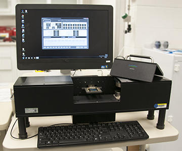
Image of Ecopia HMS-5500 Hall Effect measurement system
The HMS-5500 Hall Effect measurement system is used to measure electrical resistivity, carrier density, and mobility of semiconducting materials. The system is easy to load and is fully automated.
Specifications/Capabilities
- Resistivity measurements: 10-4 to 107 Ohms-cm
- Mobility measurements: 1 ~ 107 cm2/Volt-sec
- Concentration: 107 ~ 1021 cm-3
- 0.55T nominal magnetic flux density
Usage Information
Supported Sample Sizes
- 5 x 5 mm up to 15 x 15 mm
Recommended Substrates/Restricted Materials
- Semiconducting/None
Typical Applications
- Measure carrier concentration
- Measure mobilities and resistivity
Created March 22, 2017, Updated March 4, 2025