
Official websites use .gov
A .gov website belongs to an official government organization in the United States.
Secure .gov websites use HTTPS
A lock (
) or https:// means you’ve safely connected to the .gov website. Share sensitive information only on official, secure websites.
Silicon-based single electron current standards
Summary
We are working to fabricate and perform low-temperature measurements of CMOS-compatible single electron devices in silicon which could be used as a standard of electrical current. Our goal is to produce a current of about 10 nA from about 100 single electron devices operating in parallel with a relative error rate below 10-8.
Description
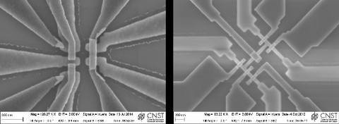
Single electron devices with integrated charge sensors in two different architectures. Left: Polycrystalline silicon gates on a bulk wafer. Right: Mesa-etched silicon-on-insulator (SOI) wafer with polycrystalline silicon gates.
Our devices can manipulate and trap a single electron in a quantum dot through the application of voltages to electrostatically controlled tunnel barriers. By cycling these voltages appropriately, we are able to sequentially pump one electron at a time through the device. To produce a current standard we run the cycle at a frequency, f, to produce a current, I=ef. This forms the basis for an electrical current standard based on the charge of the electron, a fundamental constant, and the frequency at which we run the device. When 2 or more devices are operated in parallel the current is multiplied by the number of devices. By parallelizing about 100 devices and operating at about 1 GHz we could produce a current of about 10 nA.
Efforts include:
- Understanding the source of different error mechanisms for pumping electrons. For instance, during a cycle we could erroneously pump zero or two electrons rather than one causing the current to deviate from I=ef.
- Fabricating and measuring devices with minimal defect densities to eliminate any drift in a device's operating point as well as minimizing differences in each device's response to gate voltages.
- Evaluating the effectiveness of different device architectures and designs as they relate to error rates.