
Official websites use .gov
A .gov website belongs to an official government organization in the United States.
Secure .gov websites use HTTPS
A lock (
) or https:// means you’ve safely connected to the .gov website. Share sensitive information only on official, secure websites.
Summary
Key industrial optics-based measurements of nanoscale structures are growing ever-more complex due to increasing device and materials complexity. To meet these challenges, we are seeking to rigorously integrate advances in machine learning into expert measurement strategies using optical microscopy and electromagnetic modeling to yield quantitative measurements with uncertainties of dimensions more than an order of magnitude below traditional resolution limits. Applications enhanced from these methods will include defect inspection and critical dimension metrology for nanoelectronics.
Description
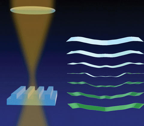
Schematic of unresolved imaging of a periodic structure. Extracting deep-subwavelength information from such images requires mastery of several techniques; this project seeks to integrate machine learning for metrology.
This project extends optical capabilities for the characterization of nanoscale devices as they increase in complexity, with challenging new materials properties, thicknesses, and length scales that challenge simplistic applications of the fundamental equations of electromagnetism.
Critical dimension, structure, and materials information are contained within optical scattering, even from unresolvable periodic structures. Geometries of such structures are recoverable through establishing parameters for the structure (width, height, etc.) and utilizing physics-based electromagnetic modeling to pair the expected signal to be obtained at a certain height & width with intensity and/or phase information measured optically. Through non-linear regression methods, we not only yield parametric values but also parametric uncertainties, which are central to quantitative metrology. At times, optical methods cannot easily distinguish between changes in height from changes in width, as each may affect the intensity similarly. This parametric correlation is important as it increases the parametric uncertainty. By introducing prior knowledge (e.g., a measurement from another tool) through NIST-pioneered “hybrid metrology,” the effect of these correlations on uncertainty can be reduced.
Envisioning the nanoelectronics of the next decade, not only will existing methods for solving this “inverse problem” need to be improved, but metrologists must also understand and harness quantitatively the potential offered from rapid advances in artificial intelligence. As alternative approaches are being developed to obtaining the desired parameters without non-linear regression, serious questions must be raised concerning accuracy and uncertainty analysis. This project seeks to develop quantitative approaches for interpreting optical scattering and imaging of nanoscale devices though the use of machine learning (ML).
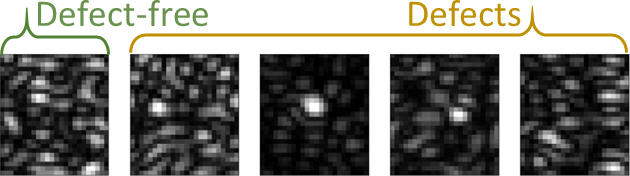
The project’s initial concentration and challenge is to develop ML competency, achieved through the development of advanced ML for the detection and potential classification of patterned defects. Patterned defects are a $1 billion per year problem for the semiconductor industry and inspecting defects with light yields four potential outcomes – two are true, accurate determinations (defect/defect-free), one is the false classification of a defect-free image, and one is the false classification of an actual defect. The ramifications are significant between these two false cases, and the ML must be attuned to these consequences. Our initial investigations have recently been published and work is ongoing on this grand challenge of semiconductor metrology.
The main emphasis of the project is the ML-aided measurement of these critical dimensions with uncertainties. This fundamental problem of uncertainty in ML is quite contemporary. We seek the potential reconciliation of known ML methods with our existing understanding and definitions of uncertainty. Not only optics-based measurements but other model-based measurements require a thorough investigation of the connections that exist among ML-produced parametric mean values, parametric correlations, and parametric uncertainties.
Major Accomplishments
2020
- Reported comparisons among conventional (e.g., library lookup) and machine learning (e.g., radial basis function, Gaussian processes) approaches to solving the inverse problem of optical scattering to determine sub-wavelength dimensions, also known as optical critical dimension (OCD) metrology. Identified limits of Gaussian process regression (GPR) versus RBF approaches thus far.
- Advocated for greater use of atomistic models such as tight-binding calculations or density-functional theory as potential approaches for understanding the dielectric function (and thus optical constants) for emerging materials at near-atomic scales, which may be both thickness dependent and anisotropic.
2019
- Successfully compared two different ML techniques, linear classifiers (LC) and convolutional neural networks (CNN), to simulated defect images with line-edge roughness, a known cause of false defect detection. CNN proves to extend detectability and enhance classification to these defects, even those that are more than 20 times smaller than the inspection wavelength.
- Presented to the industry how CNNs can be improved not only in their architecture but also tailored to the specific challenges of defect inspection through more specialized performance metrics. These advances may lead to more cost-efficient measurements by adjusting the decision threshold to minimize the number of wrong defect detections.
- Revealed through simulation how the form-dependent optical response changes as the wavelength approaches the periodicity by realistically comparing five wavelengths numerically, with surprising results at 47 nm wavelength due to its wavelength-dependent optical properties. This study is the physics-based foundation upon which our machine-learning approaches are subsequently tested.