
Official websites use .gov
A .gov website belongs to an official government organization in the United States.
Secure .gov websites use HTTPS
A lock (
) or https:// means you’ve safely connected to the .gov website. Share sensitive information only on official, secure websites.
Summary
The interruption of crystal structures by just a few intentional or unintentional mistakes, or bonding errors, can greatly impact the macroscale behavior of solid-state materials. However, it is incredibly difficult to study these crucial bonding errors in their naturally occurring state. More specifically on the nanoscale, there are huge gaps in understanding how a dilute number of bonding errors interact with nearby adjacent bonding errors as well as the local environment where they occur. Realization that these bonding errors almost always contain some number of unpaired electrons with consequent magnetic moments allows one to invoke electron spin resonance methods to begin to unravel the details of these all-important bonding errors with the goal of eventually controlling their absence or presence. However, electron spin resonance methods typically involve measurements of larger ensembles of unpaired electrons which are trapped in these bonding errors. The aim of this project is to develop measurement tools which are instead sensitive to more dilute densities of the electron spins trapped in these bonding errors. The strategy involves merging atomic force microscopy imaging tools with highly sensitive electron spin resonance detection schemes to “image” small numbers of these bonding errors in their naturally occurring state. This approach has implications to the fundamental solid-state physics which govern charge transport in a variety of inorganic and organic crystals as well as their participation in quantum state variable manipulations.
Description
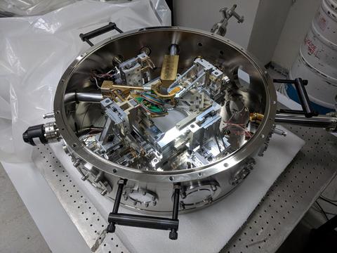
Prototype cryogenic atomic force microscope system with nanoscale electron spin resonance capability
While the characteristics of the unpaired electrons which are trapped in these bonding errors have a dramatic impact on the macroscale material properties, observing these same unpaired electrons has proven quite difficult. These unpaired electrons are transient in time, temperature, and pressure and are largely influenced by the local (atomic-scale) electric and magnetic fields which are omnipresent at the nanoscale. Recent efforts to pin down these slippery characters have turned toward a variety of nanoscale imaging techniques with varying degrees of success. In this NIST research effort, a variation of atomic force microscopy is being developed to image induce spin transitions on small numbers of unpaired electrons at the surface of a variety of materials systems. These material systems include everything from two-dimensional material stacks to organic and inorganic semiconducting crystals. In all cases the atomic-force microscopy tip is used to supply high frequency magnetic fields which induce spin state transitions. The same atomic-force microscopy tip is also used to detect local changes in impedance due to these spin state transitions. This transmit-receive antenna approach allows one to image surfaces with a wide variety of conductivities. Detection of the minute changes in local impedance is aided by a variety of NIST custom-built microwave interferometry circuits which interface directly to the antenna tip.
This atomic force microscopy imaging approach resides inside a high-vacuum chamber which permits measurements from cryogenic temperatures (< 10 K) up through temperatures which exceed room temperature (> 450 K). The chamber is coupled to a super conducting out of plane magnet which is needed to polarize the unpaired spins in preparation for the tip-based spin transitions. The system also includes an additional non-antenna atomic force microscopy probe as well as several coarse probes which can be used to supply local electric potentials to the materials under test. NIST has established an ongoing effort to realize this unique imaging capability which will have obvious impacts in imaging/probing the fundamentals of charge and spin transport in a variety of semiconducting and insulating materials systems for use in advanced device technologies, optoelectronic technologies, memory technologies, and the emerging needs of the quantum information science revolution.