
Official websites use .gov
A .gov website belongs to an official government organization in the United States.
Secure .gov websites use HTTPS
A lock (
) or https:// means you’ve safely connected to the .gov website. Share sensitive information only on official, secure websites.
Summary
Integrated photonics uses micro-and nano-fabrication techniques to develop compact devices that can replace bulk optics. Low size, weight, and power (SWAP) often leads to a reduction in cost. Integrated photonic devices are an exciting way for NIST to disseminate devices with high performance that can function as a calibrated light source.
Description
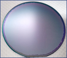
Photograph shows a 76 mm III-V epilayer wafer-bonded to a tantala substrate. The GaAs substrate has been chemically etched away, and the wafer is ready for further fabrication.
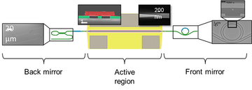
The Integrated Photonics Project utilizes heterogeneous materials integration to demonstrate novel optoelectronic devices such as semiconductor lasers, wavelength converters, and polarization rotators with compact form. We use materials including silicon, silicon dioxide, tantalum pentoxide, and AlGaAs to enable various functionalities.
III-V semiconductors such as GaAs have very large nonlinear optical coefficient, even larger than that of lithium niobate. Molecular beam epitaxy (MBE) is used to deposit alloys of AlGaAs and InGaAs on GaAs substrates with precise thickness control. Combined with microfabrication techniques such as wafer bonding and plasma etching, engineered structures with desired nonlinear optical properties can be engineered. Applications include narrow linewidth semiconductor lasers, monolithically integrated optical parametric oscillators, low energy f-2f converters for fceo detection of frequency combs, and various other types of devices.
Papers
Eric J. Stanton, Jeff Chiles, Nima Nader, Galan Moody, Nicolas Volet, Lin Chang, John E. Bowers, Sae Woo Nam, and Richard P. Mirin, "Efficient second harmonic generation in nanophotonic GaAs-on-insulator waveguides," Opt. Express 28, 9521-9532 (2020)
Eric J. Stanton,Lin Chang, Weiqiang Xie, Aditya Malik, Jon Peters, Jeff Chiles, Nima Nader, Gabriele Navickaite, Davide Sacchetto, Michael Zervas, Kartik Srinivasan, John E. Bowers, Scott B. Papp, Sae Woo Nam, and Richard P. Mirin, “On-Chip Polarization Rotator for Type I Second Harmonic Generation,” APL Photonics 4, (2019).
Jeff Chiles, Nima Nader, Eric J. Stanton, Daniel Herman, Galan Moody, Jiangang Zhu, J. Connor Skehan, Biswarup Guha, Abijith Kowligy, Juliet T. Gopinath, Kartik Srinivasan, Scott A. Diddams, Ian Coddington, Nathan R. Newbury, Jeffrey M. Shainline, Sae Woo Nam, and Richard P. Mirin, "Multifunctional integrated photonics in the mid-infrared with suspended AlGaAs on silicon," Optica 6, 1246-1254 (2019)
Nima Nader, Abijith Kowligy, Jeff Chiles, Eric J. Stanton, Henry Timmers, Alexander J. Lind, Flavio C. Cruz, Daniel M. B. Lesko, Kimberly A. Briggman, Sae Woo Nam, Scott A. Diddams, and Richard P. Mirin, "Infrared frequency comb generation and spectroscopy with suspended silicon nanophotonic waveguides," Optica 6, 1269-1276 (2019)
Major Accomplishments
Demonstrated infrared frequency combs from 2.0-8.8 um using dispersion-engineered, suspended silicon waveguides.
First demonstration of a suspended AlGaAs waveguide platform for chip-scale, nonlinear optics.
Developed fabrication processes for full wafer bonding of III-V semiconductors to dielectrics for active integrated photonics, including the demonstration of CW semiconductor lasers around 1000 nm.