Summary
A suite of tools for high-throughput synthesis and characterization of thin-film combinatorial libraries
Description

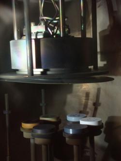
There are many materials science problems that don’t have good modeling frameworks and exist in large design spaces. In these domains the best approach is to rapidly acquire data. To achieve this we can deposit metallic alloys as thin films with a range of composition (or less commonly processing parameters). In our group, we achieve this through use of combinatorial co-sputtering, which uses the natural deposition rate variation of three non-coincident sources to create a composition gradient in the resulting thin-film. We also have a variety of automated tools to characterize these films, both within the group or in other parts of NIST. We use x-ray fluorescence mapping and x-ray diffraction mapping to measure the composition and crystalline structure respectively as a function of position. We have demonstrated EXAFS mapping at the NIST BMM beamline at NSLS-II We also have access to a variety of tools to map functional properties. Within our group, the scanning droplet cell can be used to map the corrosion properties of the film. Collaborators in the Nanomechanical Properties Group have developed tools to map both the room and high temperature thermopower and thermal conductivity of these films. Probes for electrical conductivity are also available at CNST.

