
Official websites use .gov
A .gov website belongs to an official government organization in the United States.
Secure .gov websites use HTTPS
A lock (
) or https:// means you’ve safely connected to the .gov website. Share sensitive information only on official, secure websites.
Summary
This project provides new measurement methods, property data and simulations for areas critical to US manufacturing, describing the mechanisms responsible for mechanical behavior. The mechanical behavior of virtually all materials (from nanostructures to bulk structural steels) depends upon processes active at the nanoscale; we provide critical evaluations of the sensitivity of nanomechanics test methods to uncontrolled experimental conditions and develop new measurement methods for probing elastic strains, defect structures and crystallographic orientations at the nanoscale within nanostructured materials and devices.
Description
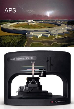
• We have provided general users from industry, academia and national laboratories with a completely new class of X-ray imaging techniques for materials studies (ultra-small-angle X-ray scattering imaging), that we developed from basic concept to DOE-supported operations at the Advanced Photon Source (APS).
• General users at the APS will benefit from a new robust measurement capability for measuring elastic strains, defects and crystallographic orientations from buried nanoscale sample volumes within nanostructured materials and devices.
• NIST is working hard to provide nanoscale researchers and engineers with a nN-level force standard. Quantum-level simulations of gold nano-wire deformation have confirmed that this system is suitable for an intrinsic force standard.
• All users of nanoindentation will benefit from critical, quantitative evaluations of the method's sensitivity to unavoidable variations in indenter tip shapes and sample roughness.
Approach
The mechanical behavior of device materials during processing, assembly, use and failure is a critical factor for nearly all industrial products. This behavior is generally determined by complex nanoscale processes such as the evolution of local stress concentrations, defect propagation, local slip, and delamination. Targeted quantitative measurement and modeling techniques are critical for making new products affordable and reliable.
Topic areas include: 1) using quantitative, experimentally validated computer simulations to evaluate nanoindentation and nanowire failure, and 2) developing and using new spatially resolved synchrotron X-ray diffraction and small-angle scattering measurement techniques for probing elastic strains, defect structures, crystallographic orientations and densities at the nanoscale within nanostructured materials and devices.
For example, USAXS imaging is now being used at the APS for studying subjects as diverse as the self-assembly of conductive-nanowire networks and the distribution of second-phase particles in artificial rubber materials.
Major Accomplishments
High impact and effective dissemination of NIST measurement capabilities can be achieved by directly incorporating these experimental techniques into national user facilities such as the DOE-operated APS. One such measurement method is USAXS imaging which was conceived by NIST scientists in 2000. Since that time, the required instrumentation, experimental techniques and underlying theory have been developed and implemented. USAXS imaging is extremely sensitive to density changes in materials and provides quantitative measures of the sizes, shapes and spatial arrangements of the underlying microstructural features. In 2005, USAXS imaging was added to the APS ten year tactical plan with the highest possible priority. It has now been incorporated into a new imaging beam line and the first DOE-supported user experiments (with no NIST involvement) were conducted in November, 2007. Continued development of USAXS imaging is supported through a Partner User Agreement between NIST and DOE.
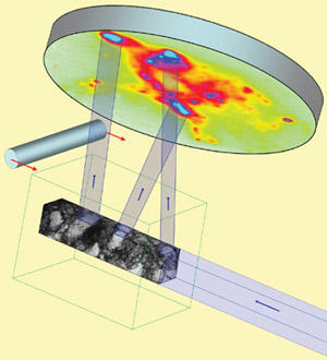
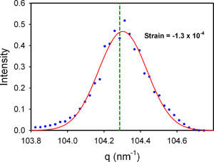
In a similar vein, NIST staff are collaborating with researchers from Oak Ridge and Argonne National Laboratories to develop a robust measurement capability for measuring elastic strains, defect densities and crystallographic orientations from buried sample volumes smaller than (200 nm)3. This technique was first utilized in 2006 to measure elastic strains within individual dislocation cell interiors in plastically deformed Cu with a spatial resolution of (500 nm)3 (see Publications). The experimental methods have since been greatly refined, and full diffraction line profiles can now be obtained from contiguous buried sample volumes. For example, in a recent experiment, diffracted intensity from a 0.07 μm3 sample volume, buried 11 μm deep in a deformed Cu sample, was isolated and analyzed. This sample volume contained a single dislocation wall separating two low-dislocation-density regions. Independent line profiles were extracted from all three sub-volumes allowing quantitative determination of local elastic strain, dislocation density and angular misorientation. The figure below shows the diffraction line profile from the dislocation wall. The location of the peak gives the average elastic strain and the width of the peak is determined by the dislocation density.
On a separate topic, current methods for measuring local mechanical properties at the nanoscale are sensitive to nanoscale variations in the sample/probe geometry, but the magnitude of this sensitivity is largely unknown. NIST researchers used atomic force microscopy to characterize the 3D shape of a nanoindenter tip and used finite element modeling (FEM) to simulate a nanoindentation experiment. An "effective radius" for the tip was determined from the simulated data, and FEM simulations were conducted from this idealized geometry for comparison with those from the measured geometry. The differences in the stress distributions provide a quantitative measure of the experimental stress uncertainties caused by the non-spherical shape of the tip.
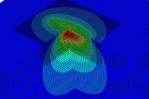
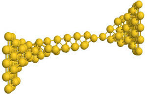
Finally, plastic deformation of gold nanowires has received considerable attention recently due to their ability to form single atom chains which results in quantized conductance. NIST has identified the breaking of such nanowires as a likely candidate for a much needed intrinsic force standard for very small loads, and accurate quantum-mechanics-level simulations have been used to explore the deformation behavior over a wide range of deformation conditions. The figure below shows the atomic configuration of a stretched gold nanowire that was simulated using density functional theory. It was found that single atom chains are easily formed and that the breaking force of these chains is extremely consistent at (1.53 ± 0.02) nN, confirming that this system is suitable for an intrinsic force standard.
Associated Product(s)
Project Summary (PDF)