Official websites use .gov
A .gov website belongs to an official government organization in the United States.
Secure .gov websites use HTTPS
A lock (
) or https:// means you’ve safely connected to the .gov website. Share sensitive information only on official, secure websites.
Summary
The project aims to develop the metrology for accurate, reliable characterization of nanostructures using the deep ultraviolet (DUV) and extreme ultraviolet (EUV) imaging microscopy with sophisticated illuminations for efficient manufacturing of the next generation computing devices. The research scope covers Scatterfield Imaging Microscopy and Computational Nanoscale Microscopy including Reflective Fourier Ptychography, Lensless Ptychography for characterization of 3D nanoscale structures with sub-nanometer sensitivity and uncertainty. These measurements are developed through manipulation of illumination scheme, frequency domain expansion, phase modulation, polarization variation and quantitative phase retrieval algorithm with high reliability.
Description
Novel optical nanoscopy techniques using deep-ultraviolet (DUV) and extreme-ultraviolet (EUV) laser sources are developed to characterize nanostructures with high dimensional sensitivity and low uncertainty for advancing the semiconductor devices manufacturing process. The illumination beam is manipulated at the conjugate back focal plane to form selective intensity/phase distributions at the image/Fourier planes which correspond to the spatial and frequency domain. The parameters of the nanoscale features such as linewidth, pitch, height, and defects in array are characterized through the illumination engineering in multimodal methodologies.
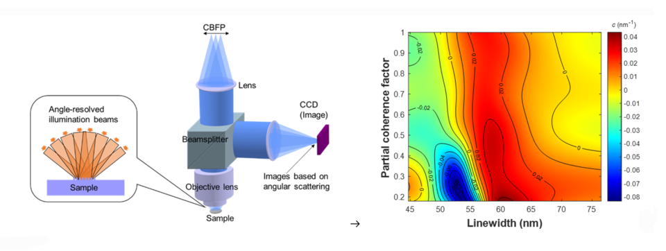
Model-based scattered image analysis: the illumination light is controlled by placing various apertures or phase plates or scanning an aperture at the conjugate of the back focal plane of the objective, so that the scattered light at the nanostructure sample can be traceable to obtain the accurate sample parameters and the optimized sensitivity.
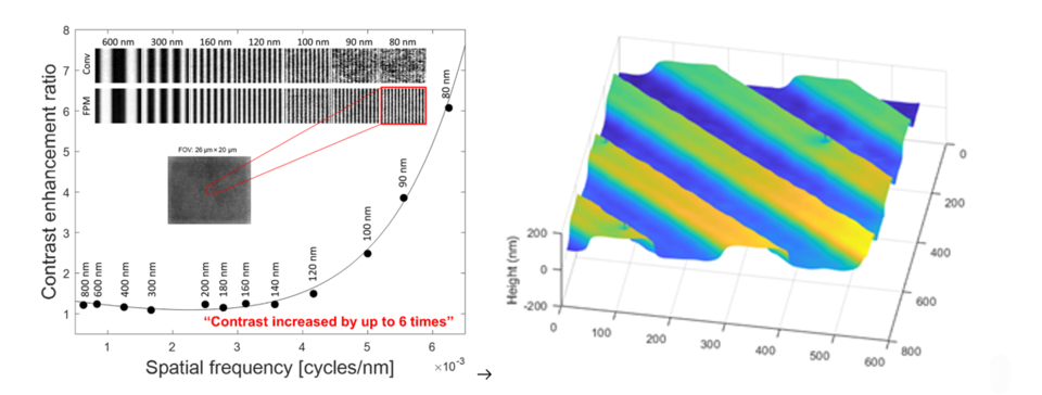
Computational nanostructure imaging: DUV/EUV reflective Fourier Ptychographic Microscopy with scanning illumination is developed to enable 3D image reconstruction of nanoscale features by computationally extracting the amplitude and phase information with spatial frequency ranges expanded beyond the resolution limit.
Major Accomplishments
- Developed the partial coherence optimization method in scatterfield imaging microscopy for quantitative dimensional metrology, achieving 0.2 nm measurement sensitivity.
- Demonstrated nanoscale imaging with Reflective Fourier Ptychography based on the 193 nm angle-resolved illumination microscope, achieving high contrast at the diffraction limit and nanoscale 3D image reconstruction.
Additional Technical Details
Schematic of optical microscopy with angle-resolved illumination controlled at conjugate back focal plane (left) and sub-nm dimensional sensitivity map with optimized partial coherence (right).
Contrast enhancement at the diffraction limit using DUV Fourier ptychography (left) and 3D reconstructed image (right).