
Official websites use .gov
A .gov website belongs to an official government organization in the United States.
Secure .gov websites use HTTPS
A lock (
) or https:// means you’ve safely connected to the .gov website. Share sensitive information only on official, secure websites.
Summary
Provide atomic resolution imaging and analysis of complex materials and devices, while also advancing transmission electron microscopy methods.
Description
As devices continue to become smaller, more complex, and more highly integrated, atomic scale measurements of their structure, chemistry, strain, and electric field are increasingly crucial for device design, reliability, and optimization. The aberration-corrected scanning transmission electron microscope (STEM) is one of the most powerful tools for studying materials with sub-nanometer resolution. In addition to high resolution imaging, state of the art instruments provide atomic scale mapping of chemical composition, crystallographic orientation, strain, medium range order in amorphous materials, and magnetic field. 4D-STEM is also emerging as a method to map electric field and charge density.
HIGHLIGHTS
Novel Instrument Calibration
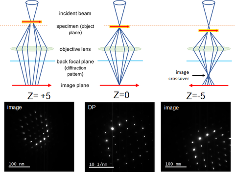
Accurate polarity determination is of growing importance for compound semiconductors and other noncentrosymmetric materials of technological interest. Convergent beam electron diffraction (CBED) is a technique commonly used to determine material polarity but requires accurate assessment of the image – diffraction pattern rotation angle. A simple method was developed for determining this angle using the asymmetry of an off-zone-axis diffraction pattern from any crystalline material. Unlike other techniques this method does not require a standard with a known polarity orientation or shape, or even a non-centrosymmetric sample.
- Roshko, A., et al. “Simple Method to Determine the Rotation Between a TEM Image and Diffraction Pattern” Microsc. Microanal. 28 2023 doi.org/10.1017/S1431927622003543
Failure analysis
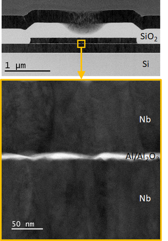
The high spatial resolution of the aberration corrected STEM makes it an ideal instrument for identifying nanoscale structural defects, which can destroy device behavior. It was, therefore, the optimal tool for examining superconducting quantum interference devices (SQUIDs) when they began to fail. Microwave SQUID multiplexers enable instrumentation of transition edge sensor arrays with hundreds of thousands of low-temperature detectors for applications in cosmology, materials analysis, and nuclear non-proliferation. NIST has been producing microwave SQUID devices for fifteen years, so it was surprising when some devices were not operational. A crucial element of the SQUID device is the <10 nm Al/Al2O3 tunnel junction. High resolution STEM imaging of these junctions revealed unexpected thickness nonuniformities in the inoperative devices (Fig 1). This issue was easily eliminated in fabrication returning the device yield to 100 %.
- Dober, B., et al. “A microwave SQUID multiplexer optimized for bolometric applications” Appl. Phys. Lett. 118 (2021). doi.org/10.1063/5.0033416
- Mates, J.A.B., et al. “Simultaneous readout of 128 X-ray and gamma-ray transition-edge microcalorimeters using microwave SQUID multiplexing” Appl. Phys. Lett. 111 (2017). doi.org/10.1063/1.4986222
- Dober, B., et al. “Microwave SQUID multiplexer demonstration for cosmic microwave background imagers” Appl. Phys. Lett. 111 (2017). doi.org/10.1063/1.5008527
- Mates, J.A.B., et al. “Demonstration of a multiplexer of dissipationless superconducting quantum interference devices” Appl. Phys. Lett. 92 (2008). doi.org/10.1063/1.2803852
Compositional analysis
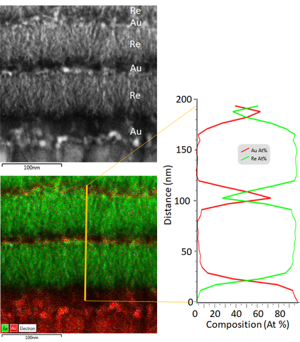
In STEM the combination of an extremely small electron probe diameter (~ 0.1 nm) and very thin specimens (~50 nm) facilitate high spatial resolution chemical analysis through X-ray and/or electron energy loss spectroscopy. When Re films electroplated onto noble metal substrates were found to have enhanced superconducting critical temperatures (up to 6 K vs 1.7 K for crystalline Re), combined STEM diffraction and X-ray chemical mapping established that the metal films were crystalline with minimal to no miscibility and no novel phases present.
- Pappas D.P., “Enhanced superconducting transition temperature in electroplated rhenium” Appl. Phys. Lett. 112 (2018). doi.org/10.1063/1.5027104
Phase identification
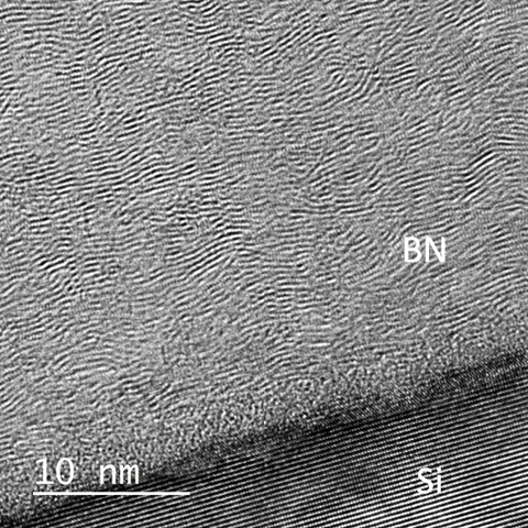
Development of novel materials and devices frequently leads to unexpected microstructures and properties. The ability to identify existing phases enables further understanding and improvement. High-resolution transmission electron microscopy (TEM) imaging of boron nitride (BN) thin films grown by electron-enhanced atomic layer deposition (EE-ALD) on Si(111) substrates is one example. The crystallinity of the films was confirmed by grazing incidence X-ray diffraction (GIXRD) analysis, which indicated they were hexagonal BN with a slightly expanded c lattice parameter. From TEM images, however, it was evident the films did not have a simple hexagonal layered structure (Fig 2). Instead, they have a graphite-like layered structure called turbostratic BN, which has a larger c lattice parameter than hexagonal BN (0.686 nm vs 0.658 nm).
7. Sprenger, J.K., et al. “Electron-enhanced atomic layer deposition of boron nitride thin films at room temperature and 100 °C” J. Phys. Chem. C 122 (2018). doi: 10.1021/acs.jpcc.8b00796