
Official websites use .gov
A .gov website belongs to an official government organization in the United States.
Secure .gov websites use HTTPS
A lock (
) or https:// means you’ve safely connected to the .gov website. Share sensitive information only on official, secure websites.
Ultra-Conformal Microprint and Ultra-Conformal Microprint Transferring
Patent Number: 11,745,493
Problem
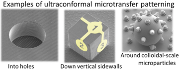
This invention is directed at solving the problem of micropatterning onto highly curved and/or uneven surfaces, transferring microscale objects from one substrate to another, as well as micropatterning onto substrate materials that are incompatible with a traditional cleanroom environment.
Invention
This invention is a new method of transferring (“transfer printing”) microstructures or micropatterns created on a first surface onto a second receiving surface, where the second surface may be highly uneven or curved or in some other way incompatible with the fabrication process requirements of the structures or patterns.
Potential Commercial Applications
Any application that requires a micropatterned / engraved / embossed surface could benefit from this technology. Applications may include: flexible electronics, such as wearable sensors, where transfer of electronic patterns is required onto flexible substrates; 3D microelectronics fabrication where micropatterning is needed on non-planar surfaces; optical engineering of materials by transfer printing them with holographic / diffractive / meta-surface optical designs; modifying object surface chemistries / properties such as hydrophobicity and drag by appropriate surface microstructuring. The technique could also be used, for example, to transfer print over common consumer objects, eg. phones, pens, etc, or onto biological surfaces or foods or drugs for sensing or anti-counterfeiting applications.
Competitive Advantage
Other transfer techniques are limited to patterning flat or gently curving surfaces and often require high temperatures and/or harsh solvents. This invention allows patterning onto arbitrary surfaces at temperatures close to room temperature and requires only water as a solvent.