Abstract
Coplanar waveguides (CPWs) with a continuous, self-aligned gap between the center trace and the ground plane are described with the additional functionality that a bridge between the two grounds is left as a crossover. The width of the gap can be made in the 100's of nm range using optical lithography, resulting in a high capacitance/unit length. This can significantly counteract the effect of high impedance due to the kinetic inductance of thin, narrow superconducting center traces. This improves yield, lowers the total impedance of the CPW, thereby making it easier to fabricate and impedance match. Furthermore, a crossover that connects the ground planes on either side of the center trace can be made at the same time as ground plane is defined and the sacrificial, self-aligned mask is removed. The centerline of the CPW is first defined using a sacrificial, self-aligned hard mask, typically SiOx. There is a small undercut at the edges of the mask. The mask is left in place while the ground plane is deposited. The ground plane is then opened up, except where a ground plane crossover of the center trace is desired, above the mask with an etch process. The mask is removed, leaving only the centerline and the ground plane material with the self-aligned gap between them. Crossovers are formed by leaving the ground plane metal above the centerline where the crossover is desired.
Patent Description
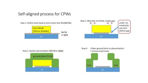
This invention enables practitioners to achieve very narrow gaps, down to 0.1 µm, on long coplanar waveguides using optical lithography. This process is shown below. In step 1, a mask is defined on top of the metallic material to be used as the center trace of the coplanar waveguide. This is referred to as a "hard mask" because it should survive the subsequent etch of the metal center trace material. The etch of the center trace is conducted in step 2. With the correct etching conditions, there will be an undercut of the center trace material from the edges of the hard mask. This undercut forms the gap. In step 3, the ground plane is then deposited on the structure and in step 4 the ground plane is then etched or planarized away above the hard mask, allowing the hard mask to be removed. This leaves a gap between the ground and the center trace material. The ground plane and the center trace should be resistant to the chemical used to remove the hard mask. The process is resistant to defects in the fabrication process and can produce structures with very small gaps that are continuous for very long structures.

Features
Benefits are: useful for fabrication for any CPW where the hard mask can be removed selectively; allows for small gaps for long lines and to control the impedance; allows for crossovers to reduce slot-line modes without extra steps; compatibility with quantum information “bare” circuits (SiOx is removed in last step); and SiOx & nitride-based superconductors have Tc>4.2K, can be used for wide range of applications.

