Problem
Integrated photonics research and manufacturing require a probe for in-line nondestructive optical testing of devices. Current optical probes require dedicated and large coupling areas in the photonic circuit. They cannot provide sufficient control over the degree, location, and direction of optical coupling, are difficult to manufacture, and suffer from sensitivity to mechanical vibration, thus making precision in-line testing of photonics difficult. NIST has invented and demonstrated a microfabricated optical probe for photonic devices that will overcome these limitations, and therefore enable such testing. The new probe can be batch-fabricated at wafer scale and can be used with existing highly developed scanning probe testing instruments.
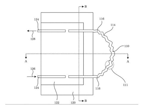
The figure below shows a microfabricated optical probe with the following components: 110 - optical loop, 111 – structured region of 110, 114 – optical waveguide, 116 – first arm of optical waveguide, 120 – substrate, 122 – optical cladding layer, 124 – first single-mode optical fiber, 126 – primary light, and 128 – output light.

Invention
Integrated photonics research and manufacturing requires a probe for in-line nondestructive optical testing of devices. Current optical probes require dedicated and large coupling areas in the photonic circuit, cannot provide sufficient control over the degree, location and direction of optical coupling, and/or are difficult to manufacture and suffer from sensitivity to mechanical vibration, making precision in-line testing of photonics difficult. We have invented and demonstrated a microfabricated optical probe for photonic devices overcoming these limitations and enabling such testing. The new probe can be batch fabricated at wafer scale and can be used with existing highly developed scanning probe testing instruments.
Features
The microfabricated waveguide loop probe reported here is small and stiff and immune to low frequency mechanical vibration. The probe is fabricated at the end of a micromechanical cantilever and used in a commercial scanning probe microscope system to control the probe-sample separation and the evanescent coupling rate.

