
Official websites use .gov
A .gov website belongs to an official government organization in the United States.
Secure .gov websites use HTTPS
A lock (
) or https:// means you’ve safely connected to the .gov website. Share sensitive information only on official, secure websites.
Problem
Miniaturized cells containing vapors of Rb or Cs can be used to detect Radio Frequency (RF) fields. In order to allow the fields to propagate to the interior of the cell without distortion or attenuation, it is important that electrically conductive materials such as silicon in the cell be minimized, as such materials can distort, and sometimes block the field entirely.
Invention
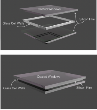
A new method for fabricating cells at the wafer level that minimizes the amount of silicon. Instead of fabricating the frame onto which glass is bonded out of silicon, we start with a glass wafer, in which holes have been etched or abrasively machined. A thin layer of polysilicon is deposited onto the top and bottom surfaces of the glass. Top and bottom glass “lids” are then bonded onto the polysilicon layer to seal the alkali atoms into the cell.
The following novel features are invented: (1) placing thin-narrow layer of silicon (Si) onto glass windows such that they can be anodic bounded to small glass cells, (2) drill holes in plates of glass in order to make single or an array of vapor cells for which windows are anodically bounded, and (3) novel process for filling and anodically bounding windows to glass cells.
Potential Commercial Applications
The sensor can be cost effectively produced using batch microfabrication and novel machines and fabrication processes Microfabricated alkali vapor cells, based on anodic bonding of silicon and glass, are the core component in a growing class of inexpensive, low-power commercial instruments. They can be fabricated in large wafers the cost per cell is significantly lower than conventional glass cells.
Competitive Advantage
The cell material is glass, and not silicon; calculations show that such cells have a much smaller effect on the RF field than a cell with silicon walls would have.