
Official websites use .gov
A .gov website belongs to an official government organization in the United States.
Secure .gov websites use HTTPS
A lock (
) or https:// means you’ve safely connected to the .gov website. Share sensitive information only on official, secure websites.
The Silicon Crystal Lattice Comparator (Delta-d) Laboratory
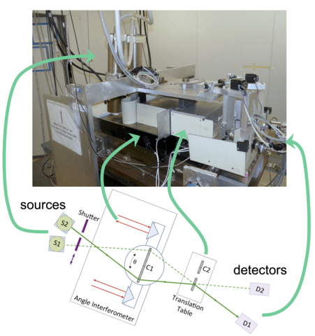
Top: photograph of the NIST lattice comparator. Bottom: Schematic. C1 is transfer standard crystal. Two crystals at C2 are the reference and actual specimen being measured. (sketch from Kessler et al.)
The silicon lattice comparator is very high-precision Laue double-crystal diffractometer which can make comparisons of the crystal lattice characteristics of a specimen crystal to those of a central reference crystal. By using the central crystal as a transfer standard, it can compare a specimen crystal to a primary-standard reference crystal to produce SI-traceable measurements of the lattice spacing of high-quality silicon. The absolute lattice constant of an unstrained crystal of intrinsic float-zone silicon can be measured to an accuracy of Δd/d < 10-8. It has been newly renovated in 2020-2022, resulting in much improved temperature stability and specimen alignment, reducing the time needed to make a comparison from days to hours.
A recent paper which covers the basics of the instrument, and a history of measurements made on it before the recent renovation, is https://doi.org/10.6028/jres.122.024. A paper is forthcoming in 2023 on the renovated instrument.
Specifications/Capabilities
The lattice comparator uses two silver KL3 (Kα) radiation beams, which are monchromated and collimated by a 450 μm thick central transfer crystal, operating simultaneously in positive and negative order, to nearly simultaneously measure the angle at which non-dispersive diffraction is achieved between the transfer and specimen crystals. This angle offset is affected by the lattice spacing difference between the transfer crystal and the specimen.
The instrument is optimized to operate on silicon specimens 455 μm thick in the analysis region, and approximately 10 mm wide. Using samples such as this, sharp pendellösung fringes appear in the diffraction pattern, resulting in the highest resolution.
However, due to the high energy the the photon source, it is capable of working with much thicker specimens, although with reduced resolution. Thus, it can be used to compare the lattice spacing and strain in a wide variety of silicon samples, including simple cut wafers.
By taking advantage of the crossed beams in various geometries, it can also measure the curvature of the lattice of silicon specimens.
Scientific Opportunities/Applications
The lattice comparator is involved in a number of measurements, one of which is described in detail at Activity on the silicon lattice comparator. The lab is not a user facility, but is always open to collaborative work which could benefit from its capabilities.