
Official websites use .gov
A .gov website belongs to an official government organization in the United States.
Secure .gov websites use HTTPS
A lock (
) or https:// means you’ve safely connected to the .gov website. Share sensitive information only on official, secure websites.
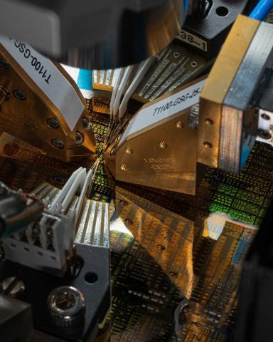
CTL uses advanced electronics technologies to develop new measurement instrumentation. Here, integrated circuits that were fabricated in a cutting-edge 25 nm Indium Phosphide high electron mobility (HEMT) process are being characterized.
With more than three decades of experience in on-chip measurements and modeling, CTL researchers have pioneered the calibration methods necessary for on-chip electrical measurements at frequencies from a fraction of a megahertz to a terahertz. These calibration methods enable the characterization of integrated electrical components, including transistors, capacitors, filters, and 3D interconnects, as well as the materials in which they are fabricated or packaged. Quantifying electronic behavior using these methods enables the manufacturer to verify the performance of the fabricated device, as well as inform and validate device models used in the circuit design process. Improvements in electrical measurements can lead to better models, more predictive design, improved manufacturability, and a better likelihood of first-pass design success.
Manufacturers and technology accelerators such as Defense Advanced Research Projects Agency (DARPA) consistently leverage CTL’s on-wafer expertise. In the fall of 2022, CTL delivered measurements and support for independent verification and validation (IV&V) of advanced microelectronics devices for three key DARPA projects.
- M3IC: CTL Researchers evaluated the final deliverables and verified new 3D heterogeneous integration of self-biased ferrite materials for integrated microwave circulators.
- COFFEE: CTL created calibration kits for the program to evaluate the response of leading-edge miniaturized filters for electronically steerable antennas.
- ELGAR: CTL provided calibrations and consultations for accurate on-wafer measurements up to 220 GHz to evaluate the high-frequency response of state-of-the-art compound semiconductor devices that are heterogeneously integrated with antenna elements for next-generation phased arrays.
Through participation in the above DARPA projects ( and others, including MMIC, Terahertz Electronics, ELASTx, DAHI and CHIPS) and other collaborations, CTL has developed measurements that characterize and model, at millimeter wave frequencies, leading-edge integrated microelectronic components, interconnects used in 3D heterogeneous integration, and advanced materials. Each project worked with industrial stakeholders including Northrop Grumman, Teledyne, Hughes Research Labs, Raytheon, IBM, Intel, AIM Photonics, Lightwave Logic, Corning, Broadpak, and Cadence. The stakeholder's applications include 5G/6G communications, biomedicine, optical communications, radio astronomy, radar, and space communications.