
Official websites use .gov
A .gov website belongs to an official government organization in the United States.
Secure .gov websites use HTTPS
A lock (
) or https:// means you’ve safely connected to the .gov website. Share sensitive information only on official, secure websites.

NIST helps semiconductor manufacturers—who are under continual pressure to make smaller, faster computer chips—reduce the time required to develop new manufacturing processes and ramp up production, and maintain high product yields.
Semiconductor fabrication starts by depositing films, so thin that they can’t be seen with a conventional microscope, on silicon wafers layer by layer so that the exact thickness can be controlled. Accurate measurements become more critical as computer chips shrink smaller: Variations as small as a few atoms can make the difference between a successful chip and a lemon.
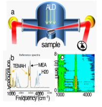
NIST’s Material Measurement Lab developed an advanced monitoring and data analysis scheme that provides equipment manufacturers with a much-improved view of the systems and chemicals that form ultrathin films. Now that we can provide this better view, industry leaders asked us to solve some intractable problems: The volatile chemicals get trapped in gas streams in ways that can’t be predicted, and they tend to degrade in the delivery system before they even get deposited. These problems can result in films with irreproducible characteristics, and reduced yield.
We also developed new ways of monitoring chemical reactions as films are deposited, giving manufacturers a better understanding of how layers of different films react with each other and helping them develop better “recipes” for films with different electrical properties.
“This work has been instrumental in evaluating new technologies, metrology, chemicals, and delivery conditions to better understand precursor vapor delivery. Optimization, and consistent control of vapor delivery for semiconductor and compound semiconductor applications is critical as feature sizes continue to be reduced in accordance with Moore’s Law.” - Bill Kimmerle, Chief Executive Officer, NSI