
Official websites use .gov
A .gov website belongs to an official government organization in the United States.
Secure .gov websites use HTTPS
A lock (
) or https:// means you’ve safely connected to the .gov website. Share sensitive information only on official, secure websites.
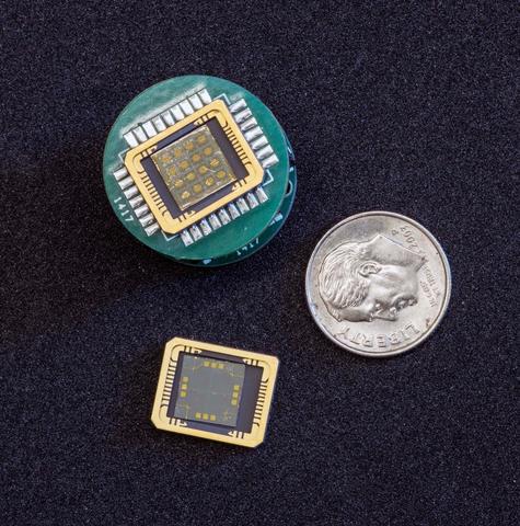
Graphene is almost transparent because it is only one atom thick. Pictured here are two graphene chips on silicon carbide. Top: an array of 16 smaller devices more typical of Quantum Hall Resistance standards. Bottom: a single device with twelve gold contacts placed near the edges. The devices are held by leadless chip carriers and can be mounted on circuit boards for ease of use.
Contrary to the popular maxim, resistance is not futile. But it is quantized: The ratings of the heat-making resistors in your hair dryer or toaster ultimately trace back to quantum mechanics.
That’s because the universal practical standard for electrical resistance is based on a phenomenon called the quantum Hall effect (QHE), in which resistance takes on perfectly exact, discrete (quantized) values under certain conditions. Those values can be measured to an accuracy of about 1 part per billion. Any metrology institute or standards lab that performs authoritative resistance measurements needs a QHE device or instruments that have been calibrated with measurements traceable to one.
QHE devices have conventionally been constructed from adjacent layers of two different, but closely related, semiconductors such as gallium arsenide (GaAs) and aluminum gallium arsenide (AlGaAs). These are, however, difficult and expensive to make. In recent years, many experiments have indicated that graphene – a one-atom-thick sheet of carbon atoms arranged in a hexagonal, chicken-wire lattice – could be used with equivalent accuracy and far fewer operational difficulties.
Now NIST researchers have devised and tested a method to produce large, homogenous graphene sheets with uniform strain optimized for QHE measurements. NIST has a long history of leadership in the field. “It’s one of the few places in the world that has successfully made standards-quality graphene, developed the technologies to make and test the devices, and done it all in-house – from raw materials to final product,” says project scientist Rand Elmquist of NIST’s Physical Measurement Laboratory (PML).
The newly reported NIST graphene is produced by placing a wafer of insulating silicon carbide (SiC, best known in abrasives and ceramics) about 2 micrometers above a bed of graphite – a form of carbon (best known as the “lead” in pencils) that is extremely heat-resistant. As the SiC is heated through several stages up to 1900 ˚C, the silicon sublimates, leaving the pure carbon behind to crystallize into graphene.
“With graphene produced by the new technique, we’re getting results that are equivalent to the current national standard, in gallium arsenide,” Elmquist says. “Recently we made a direct comparison, and got the same values to within 1 part in 109. We plan to offer a graphene QHE standard as a Standard Reference Material within a year or two. That would be the first commercial source of quantum Hall devices by themselves, and we’re also working with the private sector* to make these devices available as a complete instrument package.”
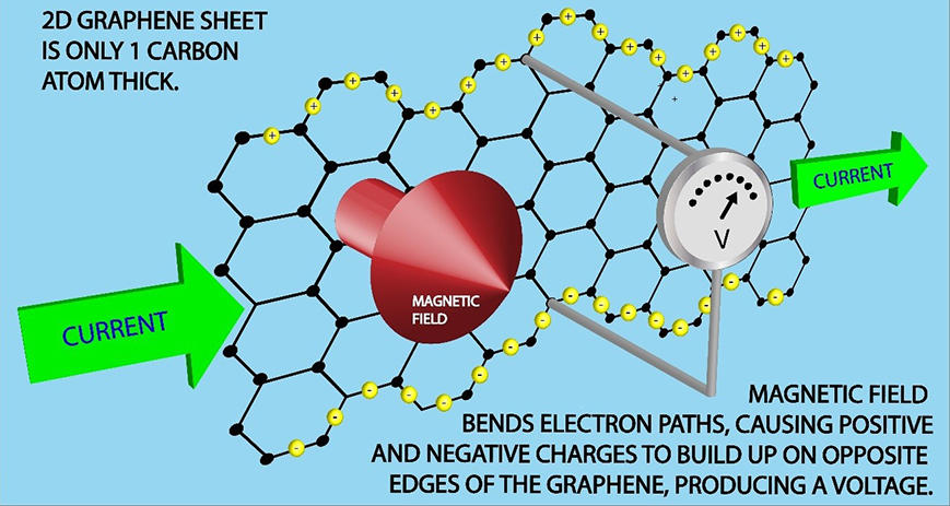
In QHE measurements, electrical current flows in a two-dimensional (2D), low-temperature conductor that has negligible thickness. Ordinarily, the current travels in a straight path and the carriers have a range of energies. But when a strong magnetic field is applied perpendicular to the plane where current flows, the field bends the electrons’ paths, forcing the positive and negative charges to detour toward opposite edges of the device. That is, there is a voltage between one edge of the sheet and the other, and the resistance between them is exactly quantized depending on the magnetic field strength due to the quantization of magnetic flux.
In conventional devices, the electrons flow in the ultra-narrow space between a GaAs layer and a ALGaAs layer, and full quantization is achieved only at high magnetic field strength and very low temperature. GaAs-type devices must be kept very cold -- 1.2 K or below, because heat can broaden and mix the energy levels – and thus the instrument requires costly, complicated cooling systems that use liquid helium.
In addition, GaAs has a comparatively small spacing between the quantized magnetic levels, and requires magnetic fields above 5 tesla (T), roughly twice the strength used in the most powerful MRI scanners. Under these conditions, the device measurements are limited to voltage levels of 1 V or below, and to small currents in the range of 20 to 80 microamperes.
“But with graphene, which is an exceptionally good conductor for a 2D material, we’ve seen full quantization as low as 2 T,” Elmquist says, “which allows us to use a much smaller magnetic apparatus that can be placed on a tabletop. Some devices are still perfectly quantized at temperatures as high as 5 K, and we have observed critical currents as high as 720 microamps, which is the highest ever observed for a QHE standard.
“If you can measure using that sort of device with its higher currents, you can accurately calibrate a room-temperature resistor of similar value, like a 1 kΩ or 10 kΩ resistor. With lower field, higher temperatures and higher current you can have a much simpler system: a closed-cycle refrigerator where you won’t need liquid helium,” he says. “By contrast, we run the NIST gallium arsenide system only twice a year because of the expense and difficulty of running the liquid helium system.”
The NIST graphene has several other advantages. Its lattice is uniform and generally lacks topological defects across areas as large as 5.6 mm by 5.6 mm – about the size of the raised electrode tip on a AA battery, and very extensive by ordinary graphene production standards. In addition, it has uniform strain on the lattice, which reduces the likelihood of moving electrons to scatter, increasing their mobility.
“It’s an exciting time for the graphene research team, and we are intensely proud of their work,” says John Pratt, Chief of PML’s Quantum Measurement Division. “They are creating a very practical standard here, one that will drive the cost of ownership and complexity of operation for quantum electrical standards down significantly.
“And this is just the tip of an iceberg for them. They have basic research results with their partners across NIST and around the country that point the way towards networks of these resistors for easy quantum-based scaling of resistance, and they have created novel diode-like junctions with applications in computing and quantum information processing, to say nothing of the optoelectronic aspects they have been considering within the general context of 2D material behaviors. Heady stuff that all spins off from the quest for a better ohm!”
* NIST’s success in device fabrication has enabled collaboration, through a Cooperative Research and Development Agreement, with Measurements International Ltd. (MIL) to commercialize a graphene-based quantum Hall resistance (QHR) standard based on graphene devices produced by PML. MIL brings expertise and experience in commercialized GaAs-based QHR standards, while PML’s quantum conductance project has expertise in fabricating and characterizing graphene quantum Hall devices to be used successfully in the QHR standards. This collaboration furthers PML’s ongoing quantum Hall device research and is aligned with PML’s mission to make primary realizations of units available to the marketplace.