
Official websites use .gov
A .gov website belongs to an official government organization in the United States.
Secure .gov websites use HTTPS
A lock (
) or https:// means you’ve safely connected to the .gov website. Share sensitive information only on official, secure websites.
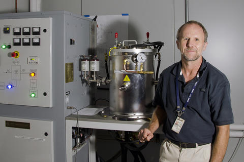
PML's Rand Elmquist with the new equipment.
Graphene – a single-layer planar sheet of carbon atoms bound in a "chicken-wire" lattice—has become the object of intense international research ever since its first isolation in 2004 propelled it into the roster of celebrity substances.
Among its many capabilities, graphene is important in metrology because it offers many advantages for studying the quantum Hall effect (QHE), and is a likely basis for the quantized Hall resistance (QHR) standard. For example, QHE plateaus in graphene can be observed at much higher temperatures and currents, and much lower magnetic fields, than devices created in gallium arsenide. But obtaining suitably large samples of the one-atom-thick carbon allotrope has been a persistent problem.
That's why in May of 2011, PML acquired a custom fabrication furnace to control the growth of sizable, high-quality graphene sheets using a promising method: cooking wafers of silicon carbide (SiC) until the silicon sublimates, leaving carbon in the form of graphene lying atop a SiC substrate. "What we're interested in is large-area graphene," says Rand Elmquist, who leads the research effort. "We want devices for our particular use that are of order millimeter-sized." That's what's needed to get the very best metrological standards, although smaller sizes are usable.
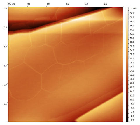
It's not yet clear what temperatures and techniques will produce the best samples. Elmquist and his colleagues have been processing SiC wafers that are about 400 µm thick at temperatures as high as 2100 °C in an argon background gas, conditions which favor homogeneous decomposition. Scanning electron microscope and atomic force microscope images (see figure below) indicate that the polished SiC surfaces reorganize spontaneously under these conditions, forming broad and smooth atomic terraces, with uniform graphene arranged in domains that are microns wide.
"You can heat the SiC in a vacuum at lower temperatures," says Elmquist. "But we're using argon at 1 standard atmosphere [1 atm = 101,325 Pa], which allows you to raise the temperature and get much larger domains. The other things that we're doing is putting two of these silicon carbide chips face to face against each other. That further limits the growth of the graphene, we think. It traps the silicon vapor between the two pieces."
The time horizon for success is uncertain, and there are many variables to manipulate. "Our eventual objective," Elmquist says, "is to make good QHR standards that are large-area devices—hundreds of micrometers or more—and have enough well-understood devices that we can distribute them to other national metrology institutes and U.S. national labs, and then maybe send the process off or teach someone to make it commercially."
"We also need to get a better understanding of what goes into making a good QHR device because the previous iterations were made from semiconductor heterostructures—gallium arsenide typically—and there you have a hundred nanometers or so of gallium arsenide above the layer that you're actually using.
Besides great basic and applied physics, graphene may also contribute very broadly to the development of beyond-CMOS logic. The Emerging Device Materials Working Group of the International Technology Roadmap for Semiconductors has directed that carbon based nanomaterials (carbon nanotubes and graphene) receive increased focus, for example as alternate channel materials. Several groups in NIST's Center for Nanoscale Science and Technology and Physical Measurements Laboratories are cooperating in their research to improve the understanding of graphene and many potential applications.
In mid-September, Willie E. May, NIST's Associate Director for Laboratory Programs, announced his decision to fund an Innovations in Measurement Science proposal titled "Measurement Length Scales to Advance Graphene Device Technologies." The researchers, from PML and NIST's Center for Nanoscale Science and Technology, proposed to "develop innovative, multi-scale methods to measure how the macroscale behavior of novel graphene devices arises from the microscopic distribution of nanoscale properties. The resulting measurement infrastructure will enable the development of graphene as an active element in a broad range of innovative device architectures to move beyond the fundamental limitations of complementary metal–oxide–semiconductor (CMOS) technology."