
Official websites use .gov
A .gov website belongs to an official government organization in the United States.
Secure .gov websites use HTTPS
A lock (
) or https:// means you’ve safely connected to the .gov website. Share sensitive information only on official, secure websites.
Researchers at the National Institute of Standards and Technology (NIST) have demonstrated a technique for growing well-formed, single-crystal nanowires in place—and in a predictable orientation—on a commercially important substrate.
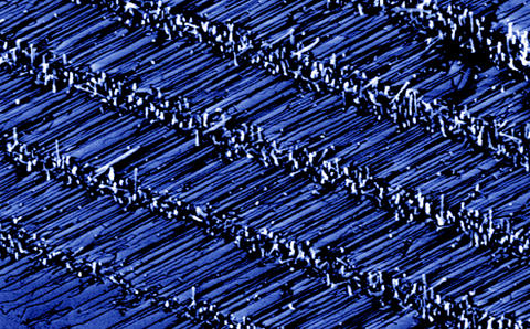
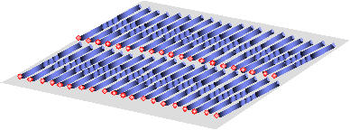
The method uses nanoparticles of gold arranged in rows on a sapphire surface as starting points for growing horizontal semiconductor "wires" only 3 nanometers (nm) in diameter. Other methods produce semiconductor nanowires more than 10 nm in diameter. NIST chemists' work was highlighted in the Oct. 11 issue of Applied Physics Letters.
Part of the vision of nanotechnology is the possibility of building powerful, extraordinarily compact sensors and other devices out of atomic-scale components. So-called "nanowires"—long thin crystals of, e.g., a semiconductor— could not only link nanoelectronic devices like conventional wire but also function as devices themselves, tipped with photodetector or light-emitting elements, for example.
An obvious stumbling block is the problem of working with components so small that only the most sophisticated measurement instruments can even track them. To date, the most successful nanowire alignment method involved growing large numbers of the rod-like crystals on a suitable base like blades of grass, shearing them off, mixing them in a solvent, and forcing them to align by either flow or surface confinement on the test substrate to orient most of the crystals in a specific horizontal direction. Further photolithography steps are required to ensure that nanowires are positioned correctly.
In contrast, the NIST technique grows arrays of nanowires made of zinc oxide, a semiconductor widely used in optoelectronics, with precise alignments. The gold "anchors" are placed with a chemical etching step and the orientation of the wires—horizontal, vertical or at a 60 degree angle from the surface—is determined by tweaking the size of the gold particles.
B. Nikoobakht, C.A. Michaels, S.J. Stranick, M. Vaudin, Applied Physics Letters, Oct. 11, 2004, Vol. 85, Issue 15, pp. 3244-3246.