
Official websites use .gov
A .gov website belongs to an official government organization in the United States.
Secure .gov websites use HTTPS
A lock (
) or https:// means you’ve safely connected to the .gov website. Share sensitive information only on official, secure websites.
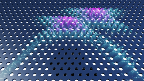
Non-linear optics relates to large power densities, which are easily achieved in small cavities, owing to the resonant enhancement. In this context, III-V semiconductor compounds emerged to be materials of choice because of their good nonlinear figure of merit. During the past few years, the fabrication of nanoscale III-V devices has improved significantly, in particular, Photonic Crystal Cavities. Thanks to their small modal volume [2] and the high Q-factor achievable [1], this type of nanoscale resonator is particularly attractive. Here, I will review non-linear interactions in photonics crystal cavities made of III-V semiconductor compounds.
First, I will present an overview of our recent results obtained in All-Optical Gates at telecom wavelengths made of InP and GaAs materials. The operation principle is based on the carrier photogeneration through Two-Photon Absorption, leading to free-carrier dispersion, modifying the refractive index, and thus the resonance shifts. The focus here is the dynamics of free-carriers, which is strongly affected by the nanoscale geometry as the diffusion length is large compared to the average distance carriers have to travel before reaching the surface. This also highlights the role of surface defects and the other chemical and physical properties of the surfaces. In this context, we developed a new model where only the surface recombination velocity acts as an unknown parameter to correctly model the dynamics of the all-optical gate [3]. Also, surface passivation was performed by Atomic Layer Deposition to obtain a conformal coating of the photonic crystal reducing by orders of magnitude the surface recombination [4]. Moreover, we addressed the issue of photo-oxidation under large optical power density thanks to this encapsulation.
Interestingly, the photo-generated carriers also modulate the resistivity of the semiconductor, and photonic crystal cavities can act as the switching element of a microwave photoconductive switch active at telecom wavelengths. Here, we show a fast response due to the surface defects, providing a large bandwidth for signal processing. Finally, resonant parametric interactions in a chain of cavities made of GaInP will be discussed. Resonant Four-Wave Mixing is demonstrated with an efficiency order of magnitudes higher than the state of the art.
[1] Zhang, Z. et al. Small-volume waveguide-section high Q microcavities in 2D photonic crystal slabs. Opt. Exp. (2004).
[2] Combrié, S., et al. GaAs photonic crystal cavity with ultrahigh Q: microwatt nonlinearity at 1.55 μm. Opt. Lett. (2008).
[3] Moille, G.,et al. Modeling of the carrier dynamics in nonlinear semiconductor nanoscale resonators. Phys. Rev. A (2016).
[4] Moille, G. et al. Integrated all-optical switch with 10 ps time resolution enabled by ALD. LaserPhoton. Rev (2016).
Agenda
1:30 PM – 2:30 PM
Speakers
Gregory Moille
Thales Research & Technology, France
Centre de Nanosciences et de Nanotechnologies, Universite Paris-Sud, France