
Official websites use .gov
A .gov website belongs to an official government organization in the United States.
Secure .gov websites use HTTPS
A lock (
) or https:// means you’ve safely connected to the .gov website. Share sensitive information only on official, secure websites.
NanoFab Tool: Oxford Plasmalab 100 Plasma Enhanced Chemical Vapor Deposition
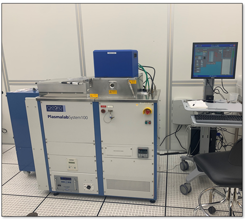
The Oxford PlasmaLab 100 is a plasma-enhanced chemical vapor deposition (PECVD) system used to deposit a variety of thin films on to a substrate material. The system uses RF power supplies to establish a plasma within the chamber which ionizes reactive gases allowing them to recombine and form a film. Due to the energy provided by the plasma, these reactions can occur at much lower temperatures than would be required in thermal CVD processes and thus provides a lower temperature alternative for depositing films such as silicon oxide or silicon nitride.
Specifications/Capabilities
- Parallel plate PECVD system with high- and low-frequency RF power supplies.
- Maximum high-frequency power: 500 W.
- Maximum low-frequency power: 500 W.
- Maximum substrate temperature: 400 °C.
- Film thicknesses ranging from a tens of nanometers to several micrometers.
- Processes supported:
- Silicon dioxide.
- Silicon nitride.
- Amorphous silicon.
- TEOS-based silicon oxide.
Usage Information
Supported Sample Sizes
- Maximum wafer diameter: 200 mm.
- Small pieces supported: Yes.
Typical Applications
- Optical waveguides.
- Silicon gate devices.
- Solar cell fabrication.