
Official websites use .gov
A .gov website belongs to an official government organization in the United States.
Secure .gov websites use HTTPS
A lock (
) or https:// means you’ve safely connected to the .gov website. Share sensitive information only on official, secure websites.
NanoFab Tool: Keithley 4200 SCS Parametric Test Station
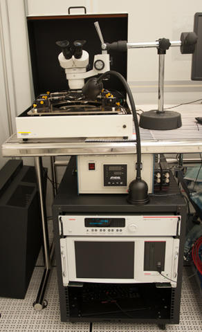
The Keithley 4200 SCS parametric test system provides in-line electrical characterization capabilities, including the ability to measure capacitance at multiple frequencies. The tool supports resistance measurements and transistor threshold measurements by supplying and measuring both DC and ultra-fast pulsed currents and voltages. A dark box enables light sensitive measurements. The enclosed chuck can accommodate substrates ranging from 150 mm diameter wafers down to small pieces and can controllably heat samples up to 300 °C.
Specifications/Capabilities
- Measure capacitance at multiple frequencies.
- Source and measure both DC and ultra-fast pulsed currents and voltages.
- Dark box for light sensitive measurements.
- Heated chuck allows measurements up to 300 °C.
Usage Information
Supported Sample Sizes
- Maximum wafer diameter: 150 mm (6 in).
- Small pieces supported: Yes.
- Maximum thickness: 5 mm.
Typical Applications
- Mobile ion concentration measurement.
- Pulsed current-voltage (IV) sweep.
- Pattern short and open testing.
- Semiconductor device threshold measurement.