
Official websites use .gov
A .gov website belongs to an official government organization in the United States.
Secure .gov websites use HTTPS
A lock (
) or https:// means you’ve safely connected to the .gov website. Share sensitive information only on official, secure websites.
Taking Measure
Just a Standard Blog

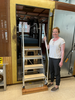
George Orji makes an adjustment to an atomic force microscope that he uses as part of a suite of instruments used for hybrid metrology, where different methods are used to capture different properties of a material. Atomic force microscopy uses a very small stylus or cantilever, something like a record player's needle, to "feel" a material's surface with sub-nanometer resolution.
What are you looking to measure? This is one of the central questions for a metrologist (a measurement scientist) and is usually answered before measurements can proceed. It is impossible to make sense of the results without knowing the measurand—the actual physical dimension or other property of the sample you want to measure regardless of the method you use.
However, the measurand could be hard to obtain if it is not defined properly or if multiple instruments are involved.
Based on the measurement needs, I know exactly what I want to measure. Nevertheless, what I want to measure and what the instrument actually “sees” could be quite different. To solve this problem, a good knowledge of the measurement model (instrument, measurement physics, data analysis, error sources and so on) for each technique is needed. But one also needs an outlook that mirrors that of a private eye: a sense of humor (the error sources are there, they are just hiding) and some patience (okay, lots of it).
For a metrologist, this is quite exciting!
The game is afoot
Methods divergence, which are when different techniques produce different results for the same measurand, have always been a problem in all aspects of metrology. In some cases, such as pitch measurements, as long as the length scales are calibrated, methods divergence are not an issue. Methods divergence are caused mostly by differences in probe-sample interaction rather than instrument calibration. Other causes include measurands that are either not well-defined or complex enough that only indirect measurements are possible. As you can imagine, the implications vary by application. Even in cases where all the measurements would be performed by the same technique, one cannot completely relax. You could be missing method-specific measurement bias and not even know it.
When other techniques are used, either as a cross-check or because they provide additional information (including prettier data or pictures), the level of work increases. When you absolutely need to use different techniques for the same measurand, things could get complicated.
In my own field, nanoscale dimensional metrology, this is increasingly the case. Some of the features being measured are now small enough, and the shapes are complex enough, that no single instrument has the resolution, speed or low level of uncertainty needed to measure every aspect we want. Absolute size is only part of the problem; the variation within and between features are equally important, and in most cases, are what we’re trying to measure. However, for nanometer-scale features, functionally important variations could easily be less than 0.5 nanometer, a few atoms’ difference. This not only pushes the limits of most instruments, but it also means that the error sources are quite different from those of larger features.
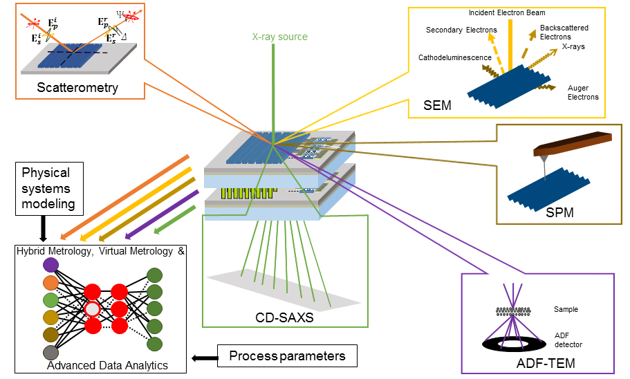
The accompanying diagram is of a stacked integrated circuit chip, along with different measurement techniques. Although there are lots of examples of methods divergence in nanometer-scale metrology, the measurement techniques needed to test the properties of stacked chips illustrate how complex things can get. On stacked chips, there are millions of features with complex geometries that are woven through the different layers, small target volumes (leading to quantum confinement, which changes the way the material behaves), and surface and interfacial roughness, among others. In some cases, the height-to-width ratio of some of the features is more than 60 to one. This is one of the cases where the measurement requirements are stringent and varied enough that no single technique has all the capabilities we need. In addition, because each layer is fully functional, measurements that need to be made after the chips are already stacked are particularly difficult since they could damage the sample.
Each instrument shown in the diagram would measure the same feature in a different way and are subject to different sets of errors that bias the measurements in different ways. For example, comparing the three-dimensional shape of a relatively simple feature such as a rectangular or cylindrical nanowire using results from different instruments is surprisingly challenging. In addition to other factors, probing errors from tip-effects (atomic force microscopy), diffraction limited optics (scatterometry), and electron scattering volume (scanning electron microscopy) would produce initial results that are different. Some techniques may not even “sense” the same information as the others. For us to understand the results, they would need to be interpreted using a valid measurement model and reported at an uncertainty level that is consistent with the model. In comparing and combining the results, how do we make sure we capture the measurand?
Hybrids to the rescue
But of course, dimensional complexity is only part of the equation. There are dozens of materials with different instrument-interaction physics. For example, proposed next-generation integrated circuit devices include materials that could be damaged by the electron beam, such as graphene, tungsten diselenide and molybdenum disulfide, among others, and devices based on atomic switches, memristors and nanophotonics that would require multiple techniques to measure. This means that available measurement techniques must be compatible with a broad range of measurement conditions or we could again risk damaging the sample.
As complicated as this confluence of factors may be, there are some exciting new (and not so new) developments that will help us understand these issues better. As you may have guessed, the main reason for this post is not to tell you that all is lost and there is nothing we can do.
One such method is hybrid metrology, which provides a framework to accurately combine results from different instruments. In cases where multiple techniques must be used to capture the measurand, each technique (such as those shown in the figure) would provide information only on those parameters it is best capable of measuring. This allows the user to extract the best measurement attribute of each technique. As such, hybrid metrology, developed here at NIST, is one of the most important measurement strategies that could be used to extend the applicability of current nanoscale metrology techniques. Hybrid metrology actually helps reduce the measurement uncertainty for all parameters, not just those provided by additional techniques. For example, in scatterometry-based feature width measurements, the analytical models include parameters where the inputs are from techniques that are best suited for such measurements. This means that such parameters are bound by their uncertainties in the model, allowing for a more stable calculation. However, this also means that each method’s deviation from the measurement model must be carefully quantified before their results could be combined.
Although great progress continues to be made in improving the capabilities of each technique, methods such as hybrid metrology allow the combined use of different methods in a way that extends the applicability of each technique.
I, robot metrologist?
Another approach is machine learning, which uses computational techniques to learn directly from data without explicitly using physical models, and can be used when evaluating a single instrument and when combining information from multiple methods. Although I was initially wary of machine learning, I’ve come to see some of its benefits. My initial skepticism had to do with what I saw as the lack of novelty in some of the underlying algorithms. Metrology has always been a computationally intensive field, and some of machine learning’s inference, prediction and decision-making methods and algorithms have been used in different aspects of metrology for a long time. What sold me was the data-driven nature of machine learning and its ability to discern previously unidentified correlations in the measurement model or between process parameters.
Sorry, error sources, you can run, but you can’t hide.
This is helpful when dealing with parameters that we cannot measure directly. In cases where physical systems modeling is computationally intensive (or some relationships are not fully understood), machine learning can be helpful. Different types of machine learning algorithms can use known input and output data to develop predictions of similar input data (supervised) or could just use input data to find hidden patterns, structures or correlations (unsupervised). Machine learning applications are quite popular. These days, it seems no conference or journal issue is complete unless it includes at least one paper on it or some other autonomous or semi-autonomous advanced analytics technique.
One caveat is that, although machine learning and other advanced data analytics techniques are extremely useful, they would complement and not replace physical systems modeling. This point cannot be overstated. To produce useful information, the data still need to be based on solid physical models and produced by instruments that are in good operating condition with the needed resolution. There is also a danger that machine learning could highlight correlations that are not relevant to the measurement model. Hence, a valid physical model is the only way to know if results from machine learning are indeed useful.
Overall, with combined use of different instruments, methods to accurately model and combine the data, and techniques to tease out hidden correlations and error sources, stacked chips, with all their methods divergence issues, may well prove easier to measure than predicted.
We will see.
* N.G. Orji, et al. Metrology for the next generation of semiconductor devices. Nature Electronics. 1,532–547 (2018)
About the author

Related Posts


Comments
A nice read. Well written.
Let's not forget the all important Bias, "Measurement Uncertainty" along with an overall "Uncertainty Budget" for all results.
Investigation, patience, more patience and a sense of humor are key to everything involved.
An excellent summary and read for anyone observing or working in these fields.
Particle size analysis is a good example here where different techniques measure something different about the particle. All answers can be right. Check out the values on the RM801x series of gold sols.