
Official websites use .gov
A .gov website belongs to an official government organization in the United States.
Secure .gov websites use HTTPS
A lock (
) or https:// means you’ve safely connected to the .gov website. Share sensitive information only on official, secure websites.
Taking Measure
Just a Standard Blog
How Extreme Ultraviolet Light Helps Give Us Smarter Smartphones and Stronger Satellites

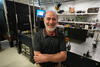
Charlie Tarrio prepares to insert a sample into an EUV reflectometer at SURF.
In 2019, after decades of effort, manufacturers used a new technology to create smartphones with individual circuit features as small as 7 nanometers (nm), or billionths of a meter, enabling them to cram 8.5 billion electronic devices known as transistors on a single small chip. Fitting more transistors in the same small space means faster, more powerful smartphones, computers and other electronic devices.
Where does the National Institute of Standards and Technology (NIST) come into play here? NIST was an early collaborator with those in the microelectronics industry who saw that it might be possible to use extreme ultraviolet (EUV) light to create electronic devices with smaller features like those we have today. This challenging goal was realized after a long, hard struggle.
Turning synchrotron radiation into a useful tool
Particle accelerators, such as the original electron synchrotron at the National Bureau of Standards (NBS, the agency that later was renamed NIST), were first developed about 80 years ago to study what was going on in the cores of atoms, known as nuclei. All such devices accelerate charged particles, a process that produces light (i.e., electromagnetic radiation), at first considered an unwanted byproduct. Back in 1961, scientists at NBS found that the light from their synchrotron, rather than being an unwanted source of energy loss, could be used to do some interesting experiments on atoms. The result was a seminal 1963 publication that showed how this now-dubbed “synchrotron radiation” could be used to uncover some never-before-observed features in how helium and other rare gases respond to light in the far ultraviolet region of the spectrum.
Having demonstrated to the world the usefulness of synchrotron radiation, NBS researchers created the first dedicated synchrotron ultraviolet radiation facility, or SURF I, to use this radiation to perform many interesting experiments and establish a new basis for calibrating various light sources and light detectors. From this unique beginning, the world has now fully invested in the use of synchrotron radiation, with over 50 synchrotron light facilities operating worldwide.

In the early 1970s, NASA used SURF I to calibrate space instruments that study the Sun. These calibrations ensured that the measurements would be accurate once the instruments were launched into space. Years later special telescopes calibrated at updated versions of SURF produced wonderful images of the solar corona at several EUV wavelengths. These EUV “pictures” helped scientists build a temperature map of the Sun.
Many such EUV measurements now being made by NASA and NOAA have more than purely scientific importance. They can serve to help in designing early warning systems for solar storms that could knock out GPS and communication links. It takes an average of eight minutes and 20 seconds for light from the Sun to reach Earth, but it takes a few hours to a few days for dangerous particles to arrive. So, if we get an early warning of a solar storm, then we could have time to prepare for it.
Using EUV to keep up with Moore’s Law
Meanwhile, in the 1980s, electronic chipmakers began to worry about how to keep up with “Moore’s law,” the roadmap that compels the microcircuit industry to constantly strive to double the number of transistors on a chip every two years or so. Making computer chips starts out with creating a pattern on a wafer of silicon in a process known as lithography (Greek for “to draw on a stone”). This is done by shining a pattern of light on a thin coating of a light-sensitive material atop a silicon wafer. The light-sensitive material is then developed to form an intricate circuit pattern.
At first, manufacturers used visible light to etch circuit patterns onto chips. The first commercially available microprocessor, the Intel 4004, came out in 1971 and had about 1,000 transistors per square centimeter. Each transistor, in turn, was made with parts having dimensions as small as about 10 micrometers, or 10 millionths of a meter.
Light waves can be imagined as waterlike ripples, with regularly repeating peaks and valleys. Just like in water waves, light’s wavelength is defined as the distance between two wave peaks. The shorter the wavelength, the closer the peaks are to each other, and the finer the patterns you can etch on a chip. In short, shorter wavelengths mean smaller transistors, and more electronic devices on the same-sized chip.
Thus, the chip manufacturers started to use light with shorter and shorter wavelengths to keep up with Moore’s law. In about 1990 they reached a deep ultraviolet (DUV) wavelength of 193 nm, which was as far as they could go using conventional optical technology.
Around the same time, several forward-looking researchers in the microelectronics industry thought that using EUV light, which has a much shorter wavelength (13.5 nm, to be exact), would be the key technology to allow the industry to continue marching forward under Moore’s Law.
The use of EUV for lithography would require a whole new optical technology: a new type of UV light source and a new type of optics. EUV required the use of “reflective” instead of the usual “transmissive” optics (that is, mirrors rather than lenses) because no material transmits light at the EUV wavelength. Also needed was a new tool environment. Instead of the tool operating at atmospheric pressure, where EUV is readily absorbed, the system required a high-vacuum environment. The job was much harder than first imagined. Many scientists and engineers familiar with microelectronics manufacturing thought it to be next to impossible to mass-produce chips with EUV.
Nonetheless, those of us at SURF collaborated with industry to develop different ways that NIST could help. We worked with large companies and industry consortia to develop instrumentation and tests for the new optics, both in terms of in their performance and their resistance to the possibly unfriendly environments they would experience within the vacuum systems that EUV lithography requires.
We privately experienced occasional doubts about whether the industry efforts would ultimately be successful. But despite the challenges, we continued to collaborate with the industry partners to overcome the many hurdles. We were glad that our contributions in the struggle to limit the degrading effect of the EUV light on the reflective optics, one of many significant problems, helped remove this barrier to progress.

EUV in space
As we have seen in NASA’s and NOAA’s study of the Sun, the importance of EUV light goes beyond chip manufacture — it includes being an essential messenger from outer space.
The Sun is constantly bombarding NASA and NOAA space satellites with radiation, including EUV light. This EUV radiation degrades important satellite components, such as optical filters. With its EUV light source, NIST can simulate five years of Sun exposure in two weeks, providing important data for protecting satellites and their delicate components.
Interest is growing in EUV and UV radiation as researchers continue to find more applications for EUV/UV light sources and optics. NIST’s research in the EUV connects some of the biggest things in the solar system to the smallest, from studies of the Sun itself to the manufacture of the tiny transistors in a cell phone. It’s great to have had the opportunity to collaborate with everyone from semiconductor manufacturers to astronomers on these projects, and we look forward to seeing and enabling future developments in EUV and UV applications.
About the author


Related Posts


Comments
I am excited reading how solar energy is being used for peaceful means. I am Reiki Therspist using Universal Energy Field for healing and wellness including long distance healing. Consider exploring Sound aspect of Universal Energy. The “OM” resonates with great cosmic vibrations so subtle all-encompassing that everything seen and unseen is filled with it. Consider exploring using Universal Energy Field for health and wellness into mainstream practice as shown by small samples of Reiki and Tuning Fork modalities. Thank You
This technology is a disruptive technology that has many more unique applications coming.
Great article. My curiosity drew me into this article because it was written for a novice like myself. I will share this with geeky friends who I know will appreciate the work you folks do as you advance our knowledge base and create all sort of cool things.
Thanks