
Official websites use .gov
A .gov website belongs to an official government organization in the United States.
Secure .gov websites use HTTPS
A lock (
) or https:// means you’ve safely connected to the .gov website. Share sensitive information only on official, secure websites.
Next-Generation Chips Require Multiple Measurement Approaches
Measurement science—or metrology—is critically important in computer chips, from design to manufacturing and quality control. The metrology requirements for next-generation computer chips are stringent and specialized. No single instrument has the speed and sensitivity that’s needed to characterize a host of complex material parameters and measure all of a chip’s dimensions—the tiny sizes and distances between its various features. Future chips will depend upon multiple dimensional metrology methods, described by NIST researchers and their collaborators in a recent article of Nature Electronics. The multiple approaches include the ones shown here.
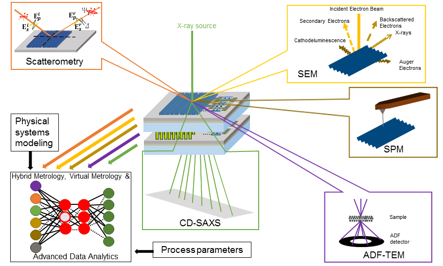
Scatterometry (top left) is an optical technique that enables measurements of sub-nanometer features of chips by scattering light (orange arrows) from the surface.
Scanning Electron Microscopy (SEM; top right) provides top-down images that yield critical parameters such as the size of microchip features.
Critical dimension small-angle X-ray scattering (CD-SAXS; center) is a technique in which x-rays non-destructively determine the average shape of the nanometer-scale structures on the chip.
In scanning probe microscopy (SPM; right), a tiny probe moves over the surface to obtain atom- and molecular-scale images of chip features. SPM technologies include the atomic force microscope (AFM) and scanning tunneling microscopy (STM).
Transmission electron microscopy (TEM) relies on interactions between a focused electron beam and the chip sample. It can produce cross-sectional images of computer chips with very fine detail. (annular dark-field TEM is shown in the diagram).
Along with these techniques, other important concepts and approaches for next-generation chip measurements include hybrid metrology (using multiple techniques to analyze the same area of a sample), virtual metrology (predictive information on chips based on process and sensor data, and in some cases actual data), and advanced data analytics. These approaches are informed by physical models of chips and the input of key parameters associated with the production process.
Paper: N.G. Orji, M. Badaroglu, B.M. Barnes, C. Beitia, B.D. Bunday, U. Celano, R. J. Kline, M. Neisser, Y. Obeng and A.E. Vladar, Metrology for the next generation of semiconductor devices. Nature Electronics. Published 12 October 2018. DOI: 10.1038/s41928-018-0150-9