
Official websites use .gov
A .gov website belongs to an official government organization in the United States.
Secure .gov websites use HTTPS
A lock (
) or https:// means you’ve safely connected to the .gov website. Share sensitive information only on official, secure websites.
Moiré Patterns Open Up More Possibilities for Quantum Information
Moiré patterns are observed throughout nature, arising from the interference between two overlaid patterns. They are especially pervasive in digital photography, where they introduce image artifacts. These artifacts result from photographing ultra-small-scale features, such as fine-print clothing or the many layers of a bird’s feathers. In a new paper appearing in Nature, NIST researchers and their collaborators have shown that it is possible to create a moiré pattern in atomically thin crystalline materials. They demonstrate for the first time how the moiré pattern affects the material’s optical properties. This has exciting implications for quantum science applications and devices at the nanometer scale.
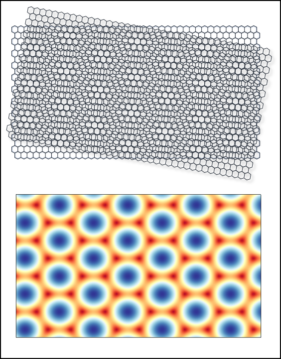
The researchers deposited ultra-thin crystalline layers of semiconductor material onto a surface. Each layer is a crystal—a regularly repeating pattern of atoms. When stacking two atomically thin sheets, the researchers showed that the periodic alignment and misalignment of the atoms in each crystal introduces a moiré pattern, depicted in the top part of the figure above. This periodic change creates a grid of low- and high-energy sites through the materials, shown in the bottom part of the figure. Red represents high energy and blue represents low energy. Each site is analogous to a valley situated between mountain peaks.
The moiré pattern thus forms a naturally ordered landscape of semiconductor quantum dots, acting as “artificial atoms” in the solid-state crystalline material. Electrons in the materials become localized and confined in the blue valleys of each quantum dot, similar to how electrons remain bound to the cores of natural atoms. The spacing between the quantum dots can be controlled by adjusting the rotational twist angle between the sheets.
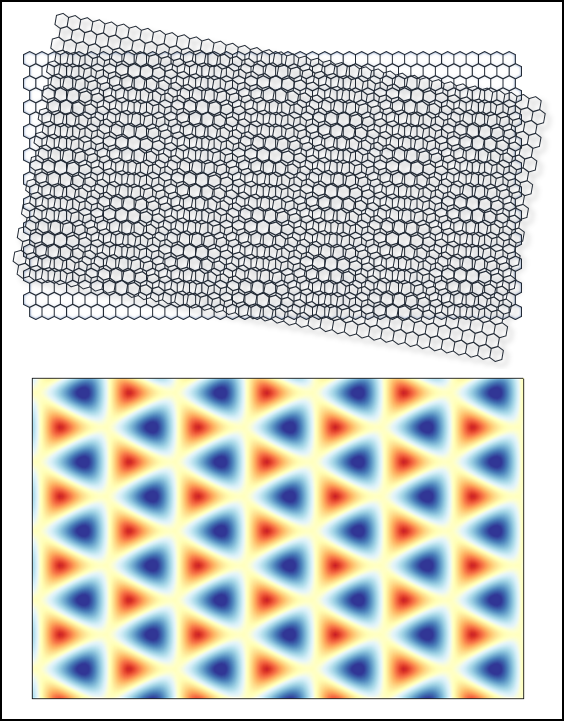
The material can also absorb and radiate visible and near-infrared light. The above figure shows that the polarization of light (its “spin”) emitted and absorbed by the material also varies periodically. Just like the array of quantum dots, this spacing can be controlled by adjusting the rotational twist angle between the sheets.
This is an exciting development for nanoscale devices relevant for quantum information applications, because these materials provide a scalable, highly configurable, and tunable platform for engineering or programming nanoscale quantum systems for storing, encoding, and transmitting quantum information. For example, with further development, this platform could be exploited for encoding quantum information in individual photons generated from each identical quantum dot in the array. For large twist angles, the spacing between the quantum dots decreases. Electrons in each quantum dot would begin to feel the presence of its neighbors, which is expected to introduce novel topological properties involving multiple particles on the edges of the material. Such topological properties can be exploited for quantum-based electronics.
This research is a collaboration between researchers at NIST and their colleagues at the University of Texas-Austin, Argonne National Laboratory, Washington University in St. Louis, the National Institute of Material Science in Japan, and Hanyang University in South Korea.
Paper: K.Tran, G. Moody, F. Wu, X. Lu, J. Choi, K. Kim, A. Rai, D.A. Sanchez, J. Quan, A. Singh, J. Embley, A. Zepeda, M. Campbell, T. Autry, T. Taniguchi, K. Watanabe, N. Lu, S.K. Banerjee, K.L. Silverman, S. Kim, E. Tutuc, L. Yang, A.H. MacDonald, and X. Li. Evidence for Moiré Excitons in Van der Waals Heterostructures. Nature. Advance Online Publication on February 25, 2019. DOI: 10.1038/s41586-019-0975-z