U.S. flag

An official website of the United States government

Official websites use .gov
A .gov website belongs to an official government organization in the United States.

Secure .gov websites use HTTPS
A lock ( ) or https:// means you’ve safely connected to the .gov website. Share sensitive information only on official, secure websites.

TEMPORAL JITTER ANALYZER AND ANALYZING TEMPORAL JITTER

Patent Number: Publication Number 2021/0311119 A1

Abstract

This is a simple method to measure the jitter, or temporal variation, of a repeated event. The method is based on simple electronic circuitry and can achieve measurement resolution on the order of hundreds of femtoseconds.

patent description

The invention is a method to characterize the temporal variation, or “jitter,” of a single-photon detector’s response with high accuracy. 
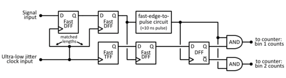
The method addresses the need to characterize single-photon detectors whose jitter is in the few-picosecond range.

The method works as follows: a single-photon detector is stimulated by a weak (less than 1 photon per pulse) periodic pulsed optical source with constant mean optical power per pulse. The optical source is synchronous with a repetitive electrical signal. The repetitive electrical signal can be controllably delayed in time by small increments over a range of time that spans the region of interest in the detector’s output. In the method, a voltage change, or “edge,” in the repetitive electrical signal is compared, using high-speed, low-jitter electronics, to the detector’s output. This comparison is carried out with a “decision circuit” that determines whether the detector’s output occurred before or after the electrical edge. The decision circuit reports the result of each comparison by outputting one of two types of countable electrical pulses that represent whether the decision circuit decided that the detector’s output arrived either “before” or “after” the arrival of the electrical edge. These output pulses are counted and the sum for each delay setting is normalized to the amount of time that each delay setting is held. As the electrical edge is stepped, using the controllable delay, across the distribution of the detector’s temporal response, the normalized counts per unit time of the pulses from the decision circuit trace out shapes that as the detector’s output occurs, at first, always after, and eventually, always before delayed voltage change. These shapes represent a convolution of the detector’s jitter and the uncertainty and variation in the decision circuit/voltage change system.

The main features of this method are that the uncertainty and variation in the decision circuit and voltage change can be low, well below 1 picosecond, the step size in the controllable delay can be small (in the femtosecond range), and the dwell time at each delay setting can be long (10s of seconds).

This method can only be used with repetitive signals; it is based on the notion that there is a large ensemble of events that are distributed in time. The method is a means to characterize that distribution. Other limitations of this method are related to stably maintaining, for each delay setting, the timing between the electrical edge and the detector’s optical stimulus. Variations of this type can be induced on a relevant scale (in the femtosecond range) by temperature changes in the circuitry, as well as other sources of instability.

Created September 19, 2022