Problem
Patent Description
This invention is a motion sensor, and the unique fabrication process required to build the sensor, that uses the strong sensitivity of plasmonic modes to geometrical parameters (e.g. gap size). The measurement technique is experimentally validated by detecting thermal motion of a variety of silicon nitride mechanical oscillators. It addresses the need for non-contact, high-spatial resolution measurement of the motion of nanoelectromechanical systems (NEMS) using an optical source.
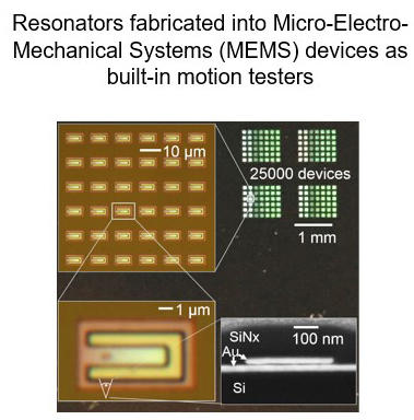
Devices based on this platform are among the first demonstrations of plasmon-based motion metrology and achieve a motion sensing figure of merit 1.5 orders of magnitude greater than existing technologies. Moreover, the fabrication process enables parallel production of thousands of functioning devices per chip, with flexibility to control mechanical resonator and plasmonic particle geometries. In contrast, existing techniques require focused ion beam processing, and are thereby restricted to serial production of individual devices, each requiring user input to fabricate. Given that the smallest lateral features patterned are 165 nm, the fabrication process can be straightforwardly adapted to 193-nm line photolithography, thereby allowing for wafer-scale batch processing of the devices. It is envisioned that the plasmonic resonators can be integrated with Doppler systems, thereby serving as sub-diffraction “Doppler phase enhancers” for improving both motion sensitivity and spatial resolution.

Invention
Two parallel gold surfaces are separated by a thin gap filled with a compliant dielectric, air or vacuum. The lateral extent (less than about 500 nm) and the shape of the gap, form a plasmonic resonator with frequency sensitive to the gap change resulting from mechanical deformation. This nanoscale device allows remote optical interrogation of local strain and mechanical motion, more sensitive and localized than Doppler vibrometry. When incorporated in MEMS, NEMS and composite materials, local strain or motion can be quantified in situ. The measurement of static as well as highly dynamic deformations (ultrasound and shock waves) is enabled.
Features
The use of plasmonic devices for motion measurement is a nascent field with the potential to greatly improve motion sensing of nanoscale systems. Given the capability to produce highly sensitive motion transducers on a chip-scale, the invention vastly improves upon the state of the art of present schemes. In addition to motion, this platform provides flexibility for future devices to be optimized for sensing a multitude of physical parameters including force, mass, stress, and heat.

