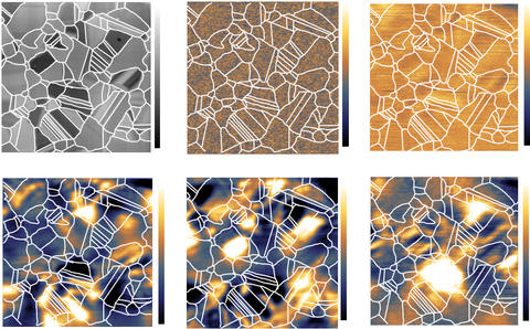
Schematic of cadmium telluride examined by the photothermal induced resonance technique.
Using two novel techniques, researchers at the National Institute of Standards and Technology (NIST) have for the first time examined, with nanometer-scale precision, the variations in chemical composition and defects of widely used solar cells. The new techniques, which investigated a common type of solar cell made of the semiconductor material cadmium telluride, promise to aid scientists in better understanding the microscopic structure of solar cells and may ultimately suggest ways to boost the efficiency at which they convert sunlight to electricity.
Even though standard methods to characterize solar cells have long proven useful in guiding their fabrication and design, these diagnostic tools “give us only a limited understanding of why the devices operate at sub-optimal efficiency,” said NIST physicist Nikolai Zhitenev. For instance, although a method known as electron-beam induced current, which analyzes samples using the beam of an electron microscope, provides data on nanoscale variations in solar cell efficiency, it gives little information on the underlying crystal defects and impurities that degrade efficiency. Two other methods, photoluminescence and cathodoluminescence, which induce light emission from the samples, provide only insufficient or indirect information on the mechanisms of efficiency losses.
To close that knowledge gap, “we’ve now developed new techniques to examine the microstructure of solar cells and demonstrated that we can visualize defects through their optical signature,” said lead author Yohan Yoon of NIST and the University of Maryland in College Park. He and his colleagues at NIST, the University of Maryland and the University of Utah described their work in a recent Nanoscale paper.
In their study, the scientists used two complementary methods that rely on an atomic force microscope (AFM). Photothermal induced resonance (PTIR) provides information on the solar cell’s composition and defects at the nanometer-size scale by measuring how much light the sample absorbs over a broad range of wavelengths, from visible light to the mid-infrared. The other method, known as direct-transmission near-field scanning optical microscopy (dt-NSOM), creates detailed nanoscale images that capture variations in the composition of the solar cells and defects in their structure by recording how much light is transmitted at specific sites within the cell. The method produces sharper images than PTIR.
The setup for PTIR, assembled by NIST researcher Andrea Centrone, resembles a finely tuned version of a Rube Goldberg contraption. First, light pulses from a laser illuminate a sample of cadmium telluride. When the sample absorbs the laser light, it heats up and expands. The expansion nudges the sharp tip of an AFM that is in contact with the sample. The tip converts the heat-induced expansion into mechanical motion, causing the cantilever on which it is mounted to vibrate. Finally, the vibration is detected by bouncing light from another laser off the cantilever into the AFM detector.

Because the extent of the cantilever’s vibrations is proportional to the energy absorbed by the cadmium telluride sample, PTIR measurements provide key information about the material. For instance, when the tip is held at one location on the sample but the wavelength of pulsed laser light is varied, PTIR generates information on the spectra of radiation that is absorbed at different points along the sample, with nanoscale resolution. When the AFM tip moves over the sample but the laser’s wavelength remains fixed, PTIR yields an absorption map of the material that reveals variations in chemical composition from one part of the sample to the other. Notably, the small size of the probe tip provides absorption information with a spatial resolution smaller than the laser wavelength used in the experiments.
In the dt-NSOM technique, light from the sharp tip of an AFM probe illuminates a small part of the sample. A photodetector in contact with the sample measures the amount of light transmitted through the material as the probe scans over the sample.
Critical to the success of the two techniques, notes Zhitenev, was not only access to an AFM, but to other advanced equipment available at NIST’s Center for Nanoscale Science and Technology (CNST), where the experiments were performed. This includes a focused ion beam that could cut slices of the cadmium telluride material a mere 350 nanometers (350 billionths of a meter) in thickness.
“Without the ability to obtain such ultrathin slices, it would not have been possible to take full advantage of the high-resolution techniques and reveal fine details of the solar cell material,” he said. The wavelengths of light used to probe the semiconductor would normally penetrate to a depth of several millionths of a meter. By cutting slices thinner than that depth, the thickness of the slices determines the effective spatial resolution of the analysis, explained Zhitenev.
The experiments showed that defects in the crystal arrangement of the material are related to impurities in the chemical composition, propagated along and from the boundaries between adjoining crystal grains. The team also demonstrated that techniques can measure the spatial variation of so-called deep defects in cadmium telluride samples. These defects, which cause electrons and holes (positively charged particles) in cadmium telluride and other semiconductors to recombine instead of generating electricity, are one of the key reasons that solar cells do not perform as well as theoretical models.
Although the new measurements are presented as a proof of concept in studying cadmium telluride, a well-characterized material, the findings “are of broad applicability and will aid solar cell research, leading to a better understanding of a variety of photovoltaic materials, and consequently, engineer them for greater efficiency,” the researchers concluded.
Paper: Y. Yoon, J. Chae, A. M. Katzenmeyer, H.P. Yoon, J. Schumacher, S. An, A. Centrone and N. Zhitenev. Nanoscale imaging and spectroscopy of band gap and defects in polycrystalline photovoltaic devices. Nanoscale. Published 12 April 2017. DOI: 10.1039/C7NR01480E.

